I once used a 74595-series shift register to expand limited MCU output ports. However, during testing where a 1 kV burst was applied to the AC power port in accordance with EN 55014-2, an issue occurred where the output data shifted by 1 bit.
Replacing the part with the TI SN74HCS595 featuring Schmitt-trigger inputs reduced the malfunction frequency, but the symptom persisted. While retaining the SN74HCS595, after adding an RC filter with a 100 Ω series resistor and a 1 nF capacitor to the CLK path, the phenomenon no longer occurred under the test conditions. This article summarizes the filter arrangement and troubleshooting process when distributing CLK to multiple ICs.
Table of Contents
Why False CLK Detection Causes Output Bit Shifts
The 74595 architecture separates the shift register from the output storage register. In the case of the SN74HCS595, serial input data is shifted on the rising edge of SRCLK, and a separate RCLK updates the output storage register. This operational structure can be confirmed in the TI SN74HCS595 datasheet.
If an unintended CLK edge is falsely detected during shifting, the data can shift by an extra bit. When RCLK subsequently updates the outputs, the shifted data appears on the parallel outputs.
Based on the symptom of the output shifting by 1 bit and the improvement achieved after applying the CLK filter, we determined that this issue was caused by burst noise coupling into the shift CLK trace and being falsely recognized as additional clock pulses.
Switching to the SN74HCS595: Frequency Reduced, but Symptom Persisted
First, we replaced the IC with the TI SN74HCS595, which has Schmitt-trigger inputs. This device incorporates Schmitt-trigger architecture on all inputs, accommodating slow or noisy input signals. TI Datasheet
A Schmitt trigger uses different switching thresholds for rising and falling input voltages. This hysteresis reduces repeated switching caused by chatter near the input threshold. However, if noise swings across both switching thresholds, even a Schmitt-trigger input can register it as a clock pulse.
In practice, after replacing the IC, the malfunction frequency decreased, but the bit-shift issue did not disappear entirely. Because input hysteresis alone was insufficient in this environment, we added a countermeasure to attenuate the noise reaching the CLK input.
Adding a 100 Ω and 1 nF RC Filter to CLK
While retaining the SN74HCS595, we inserted a 100 Ω resistor in series with the CLK signal path and connected a 1 nF capacitor between GND and the SRCLK input node downstream of the resistor.
When distributing a common CLK to multiple ICs via stub traces, applying filters individually close to the CLK input of each IC proved effective. Because noise can also couple into traces downstream of the branch point, filtering at each receiving end is essential.
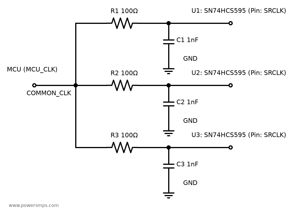
The schematic is a conceptual diagram illustrating the filter connections for each branch. The three branches represent an example configuration; DATA (SER), output latch (RCLK), power, and decoupling connections are omitted.
The connection sequence for each branch is Common CLK → 100 Ω series resistor → SRCLK input. The 1 nF capacitor connects from the input node downstream of the resistor to the local IC GND. Traces between the capacitor and GND should also be kept short.
The RC filter dampens voltage swings at the input node in response to short noise pulses, while the Schmitt trigger evaluates the filtered input signal against its hysteresis thresholds. The two countermeasures serve complementary roles.
Burst Test Results by Countermeasure
| Implementation Stage | Observed Result |
|---|---|
| Existing 74595-series IC used | Output data shifted by 1 bit during burst testing |
| Replaced with SN74HCS595 | Malfunction frequency reduced, but bit-shift symptom persisted |
| Retained SN74HCS595 + added 100 Ω / 1 nF RC filter to CLK | No bit-shift issues observed under test conditions |
The above results were verified under test conditions where a 1 kV burst was applied to the AC power port in accordance with EN 55014-2. In this circuit, the symptom that remained after swapping the IC was resolved by adding the RC filter.
Timing Considerations When Applying to Other Circuits
The ideal RC time constant for 100 Ω and 1 nF is 100 ns. Although these component values resolved the issue in this circuit, the filter impacts not only noise but also the transition edges and arrival times of the valid CLK signal. Therefore, when adapting this solution to other circuits, the following items must be verified.
- Valid CLK pulse width and input transition time: Verify that required clock conditions are still satisfied after filtering.
- Data and output latch timing: Check the setup and hold times for SER, as well as the timing margin from the final SRCLK to RCLK, against datasheet specifications.
- CLK arrival skew between multiple ICs: Account for skew caused by individual RC component tolerances and input threshold variations. In serial cascaded configurations in particular, verify data setup and hold margins between ICs.
- MCU CLK output drive loading: As the number of branches increases, the cumulative capacitive load rises; review GPIO drive capability and actual signal transmission requirements.