When designing isolated UART circuits, one must verify logic polarity, timing budgets, and drive margins across operating temperatures. In particular, when employing transistor-output optocouplers in high-temperature environments, you must verify the CTR-vs-temperature characteristic in the component’s datasheet. Assuming that output current achieved at room temperature will hold at elevated temperatures often leads to insufficient Low-level margins and communication timing failures.
Table of Contents
- 1. Critical Timing Parameters in UART Isolation
- 2. Device Selection by Baud Rate and Output Stage Structure
- 3. Active-Low Drive to Turn Off the LED During Idle
- 4. Receiver Configurations for TLP2361 and 6N137
- 5. Worst-Case Calculations for LED Current and Limiting Resistor
- 6. Always Check CTR-vs-Temperature Graphs in High-Temperature Environments
- 7. Verifying Fail-Safe Behavior Across Power and Wiring Conditions
- 8. Isolation Hardware and Communication Verification Procedure
- 9. Design Checklist
1. Critical Timing Parameters in UART Isolation
UART is an asynchronous communication protocol that does not share a separate clock line. The receiver detects the falling edge of the start bit from the Idle High state and samples the data and stop bits using its own internal clock. Because oversampling multipliers and majority voting methods differ across MCU architectures, consult the relevant UART reference manual.
Defining the rising and falling propagation delays of the isolation device as \(t_{PLH}\) and \(t_{PHL}\), respectively, the pulse width distortion (PWD) is given by:
\[PWD = |t_{PHL}-t_{PLH}|\]A uniform common delay merely shifts the entire waveform by the same amount of time. In contrast, delay asymmetry between the two propagation times, slow edge transitions under load, and jitter distort the actual durations that High and Low states are held at the receiver. When transmitter and receiver clock tolerances accumulate across the frame on top of this distortion, sampling margin degrades sharply. Misinterpreting a data bit leads to data corruption, whereas sampling a stop bit as Low triggers a framing error.
| Baud Rate | 1-Bit Duration \(T_b=1/baud\) |
|---|---|
| 9600 bps | Approx. 104.17 μs |
| 115200 bps | Approx. 8.68 μs |
As the bit duration decreases, the relative proportion occupied by the same delay asymmetry increases. Rather than fixing allowable PWD to a rigid percentage, evaluate it through a complete timing budget that accounts for MCU receiver sampling points, frame length, transmitter and receiver clock deviations, jitter, and input logic thresholds. Microchip Asynchronous Receiver Guide
2. Device Selection by Baud Rate and Output Stage Structure
| Device Family | Representative Parts | Key Design Considerations |
|---|---|---|
| Transistor-output optocoupler | PC817, TLP785 | CTR, saturation voltage, storage time, load resistance, temperature-dependent switching characteristics |
| High-speed totem-pole logic output | TLP2361 | Input threshold current, recommended LED current, supply voltage range, propagation delay/PWD, output voltage |
| High-speed open-collector series | 6N137 | Manufacturer-specific supply/temperature ranges, input current, output pull-up, Enable pin, load conditions |
| Digital isolators | ISO7721 series, etc. | Supplies on both sides, channel direction, default output state, delay/CMTI/isolation specifications |
Due to junction capacitances and storage time resulting from deep saturation, standard phototransistors do not extinguish output current immediately when the LED turns off. When the output transitions back to High, the RC time constant of the pull-up resistor and load capacitance also impedes the edge. While a high CTR benefits static DC drive, it can actually impair turn-off speed.
In practical applications handling 2400 or 4800 bps with parts such as PC817 or TLP785, operating variations must be evaluated first. Even for the exact same part, switching speed varies widely depending on LED drive current, load resistance, ambient temperature, and saturation depth. If you are designing a new UART link operating at 9600~115200 bps or higher, prioritizing high-speed logic-output optocouplers or digital isolators with guaranteed switching parameters will make achieving robust timing margins significantly easier. Toshiba Transistor Coupler Application Note
3. Active-Low Drive to Turn Off the LED During Idle
To keep the LED turned off when the UART line is in Idle High, a topology that sinks LED current into the transmitting MCU’s TX pin is employed. The current path flows from transmitter supply VDD_A → RLED → LED anode → LED cathode → MCU_TX. Here, the LED power supply must be drawn from the TX GPIO voltage domain.
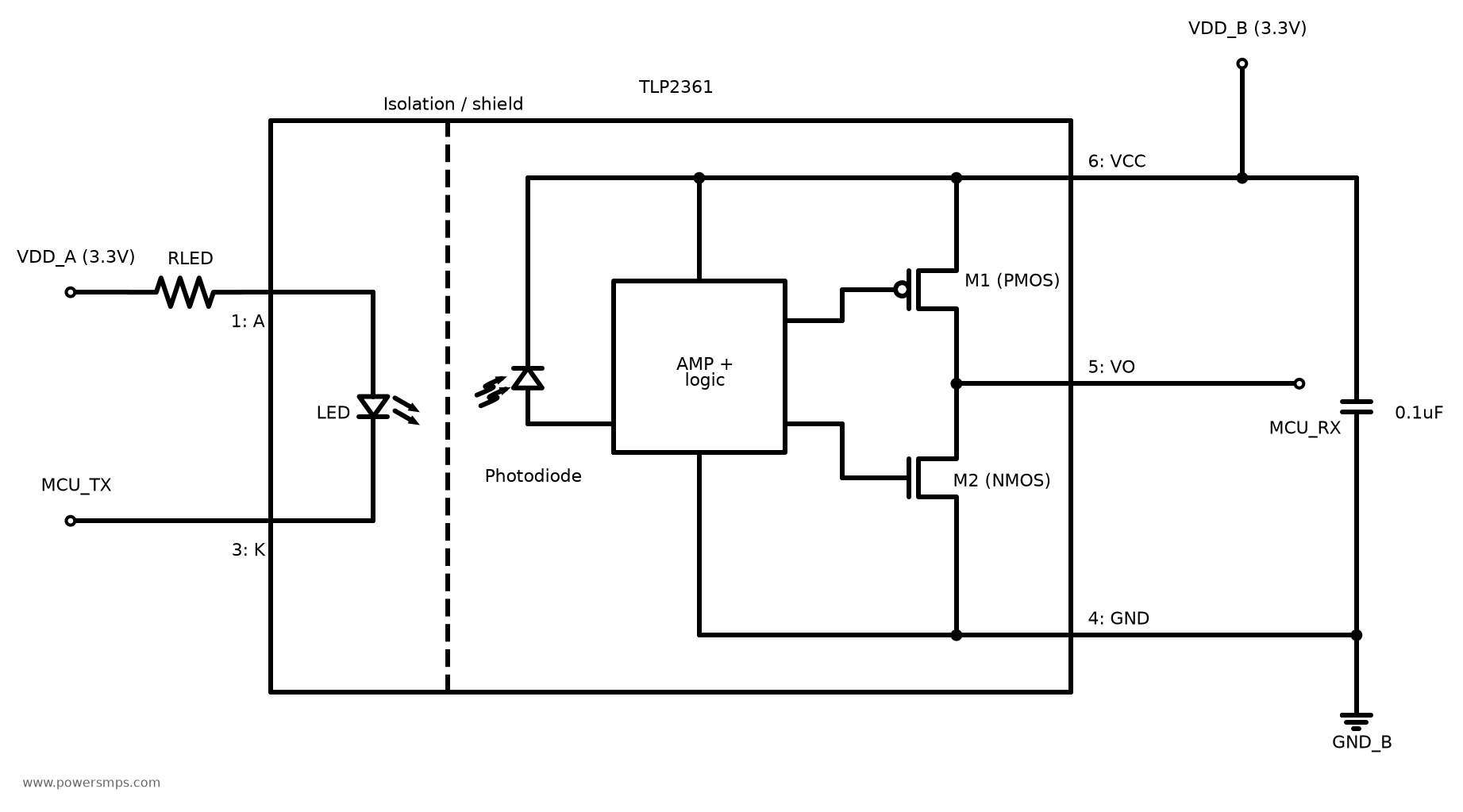
Because TX is an active output node driven by the MCU, it must never be tied directly to ground.
| MCU_TX | LED | Inverting Photo-IC Output | MCU_RX |
|---|---|---|---|
| High | OFF | High | Idle or Data 1 |
| Low | ON | Low | Start bit or Data 0 |
By pairing the Active-Low LED drive with an inverting photo-IC receiver, overall logic is delivered non-inverted from TX to RX. Because UART lines spend most of their time in Idle High, this arrangement effectively minimizes idle LED current consumption and cumulative illumination time. Note, however, that the receiver-side IC’s own quiescent supply current must still be accounted for.
If an LED connected to a 3.3 V TX pin is powered from a 5 V supply rail, residual leakage current can continue flowing through the LED even when TX is High, or current can back-feed into the GPIO internal ESD protection diodes. Therefore, verify GPIO voltage tolerance, sink current capability, load-dependent \(V_{OL}\), reset-time internal pull-up/pull-down states, and partial power-down behavior. Placing the pin in High-Z does not by itself guarantee that the LED remains completely turned off.
4. Receiver Configurations for TLP2361 and 6N137
The TLP2361 features an inverting totem-pole output, allowing its output to connect directly to MCU_RX without an external pull-up resistor. Operating from isolated receiver supplies VDD_B and GND_B, verify that guaranteed output High/Low voltage levels fully satisfy the receiving MCU’s input logic thresholds.
The pinout assigns Pin 1 to anode, Pin 3 to cathode, Pin 4 to GND, Pin 5 to output VO, and Pin 6 to VCC. Place a 0.1 μF bypass capacitor between VCC and GND, positioned within 1 cm of the pins as recommended by the datasheet. Never bridge transmitter GND_A and receiver GND_B across the isolation barrier.
The TLP2361 supports a supply voltage range of 2.7~5.5 V and an operating temperature range of −40~125 °C. The recommended LED ON current is 2~6 mA, and the maximum input threshold current \(I_{FHL}\) is specified up to 1.3 mA at 105 °C and 1.6 mA at 125 °C. Because the nominal rating of 15 MBd represents a typical figure, always review the guaranteed propagation delay and PWD specifications under your actual supply, temperature, and load conditions. TLP2361 Official Datasheet
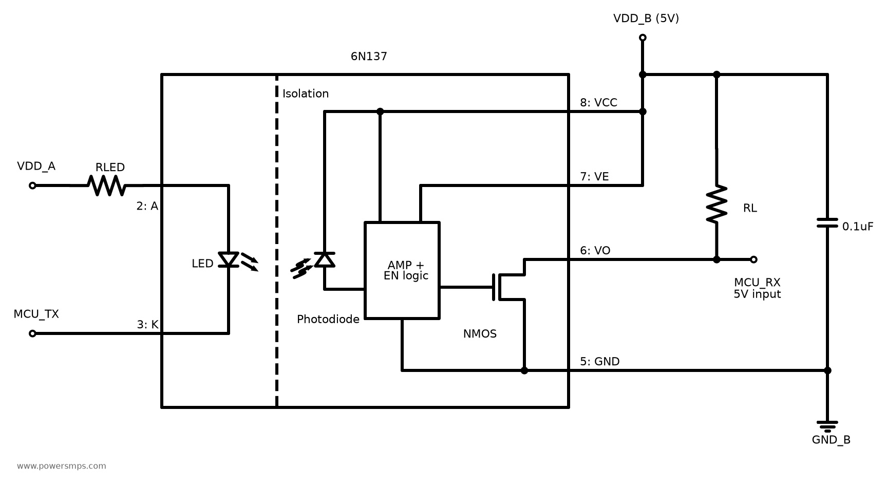
In this circuit example, the receiver-side pull-up rail is 5 V. Consequently, the receiving MCU’s RX pin must be rated to tolerate a 5 V input.
The 6N137 is an open-collector output device requiring an external pull-up resistor. For the Vishay part referenced here, the recommended VCC is 4.5~5.5 V and the operating temperature range is −40~100 °C. Because the pull-up resistance of 330 Ω to 4 kΩ and input High current of 5~15 mA represent recommended conditions in this specific Vishay datasheet, verify component specifications individually when using parts in the 6N137 family from other manufacturers.
When Enable is High, LED ON produces an output Low, and LED OFF produces an output High. Ensure the Enable pin is decisively biased to its intended active state, and size the pull-up supply according to the output transistor’s voltage rating and the receiving MCU_RX input ratings. Rather than routinely tying IC supply (VCC) and the pull-up voltage to the same rail, it is safer to evaluate the voltage ratings of each domain independently. Vishay 6N137 Official Datasheet
Selecting a smaller pull-up resistor accelerates rising edges, but increases the sink current that must be carried during output Low. The 10~90% rise time based on a simple RC model is given below; in actual circuit timing, the device’s internal storage time and propagation delays must be summed into the total delay.
\[t_r \approx 2.2R_LC_{load}\]5. Worst-Case Calculations for LED Current and Limiting Resistor
For logic-output devices, sizing calculations are based on input threshold currents and recommended LED drive levels rather than the CTR used for transistor-output devices. Incorporating resistor tolerances and supply voltage limits across the operating temperature range, the worst-case equations are formulated as follows:
\[I_{F,min}=\frac{V_{DD,min}-V_{F,max}-V_{OL,max}}{R_{LED,max}}\] \[I_{F,max}=\frac{V_{DD,max}-V_{F,min}-V_{OL,min}}{R_{LED,min}}\]When performing calculations, first verify that the numerator’s voltage margin remains strictly positive. The minimum drive current \(I_{F,min}\) must exceed the input threshold current across the full temperature range plus an aging margin, firmly placing the device within its recommended ON operating region. Conversely, the maximum drive current \(I_{F,max}\) must not violate the recommended upper limit, LED thermal derating at maximum temperature, resistor power dissipation ratings, or the maximum allowable current limits per GPIO pin and port.
In particular, the minimum, typical, and maximum specifications of \(V_F\) for the TLP2361 (1.35/1.50/1.65 V) are specified at \(I_F=2\) mA and 25 °C. At low temperatures, LED forward voltage increases, which can reduce drive current below intended levels; at high temperatures, forward voltage drops, causing current to rise. Therefore, rather than relying solely on room-temperature typical ratings or average temperature coefficients, substitute the \(V_F\) rise at the lowest operating temperature and the current increase at the highest temperature into the worst-case equations to confirm adequate design margin.
6. Always Check CTR-vs-Temperature Graphs in High-Temperature Environments
The current transfer ratio (CTR) of a transistor-output optocoupler is defined as:
\[CTR(\%)=\frac{I_C}{I_F}\times100\]CTR varies substantially with forward drive current, collector-emitter voltage, unit-to-unit variation, CTR rank, junction operating temperature, and cumulative operating lifetime. Because the emission efficiency of the LED and the current gain of the phototransistor possess distinct temperature coefficients, the peak location and slope of the CTR-vs-temperature curve differ across parts and operating points. If the circuit must operate in high-temperature environments, you must consult the CTR-versus-temperature characteristics in the component’s datasheet and identify the worst-case minimum CTR across the full operating range. Renesas Guide on CTR, Temperature, and Aging
For example, examining page 14 of the TLP785 datasheet reveals the \(I_C-T_a\) characteristic under a fixed \(I_F\) condition instead of an explicit CTR plot. Because input forward current \(I_F\) is held constant, a drop in collector current directly represents a reduction in CTR. From this curve, you can determine how sharply output current degrades at elevated temperatures and how the attenuation slope shifts with forward current magnitude. In addition, review the \(V_{CE(sat)}-T_a\) curves on the same page to track changes in saturation voltage.
Because curves in manufacturer datasheets represent typical benchmark characteristics, they differ from minimum values guaranteed across full production screening. Furthermore, active-region CTR measured at \(V_{CE}=5\) V cannot be directly applied as effective CTR in deep saturation. Therefore, cross-check the datasheet test bias, normalization references, and rank-specific minimum guaranteed CTR to conservatively establish the effective CTR at your actual operating point, adding extra margin for long-term LED light output degradation (aging).
Applying the derived effective minimum CTR allows you to estimate the available sink current that the output stage can draw under the specified \(V_{CE}\) condition:
\[I_{C,avail}\approx I_{F,min}\frac{CTR_{min,eff}}{100}\] \[I_{C,req}=\frac{V_{PU,max}-V_{OL,target}}{R_{L,min}}+I_{leak,max}\]Here, leakage current represents an additional worst-case load that the output transistor must sink. To ensure a valid logic Low voltage, the condition \(I_{C,req}\le I_{C,avail}\) must hold; thus, the static Low requirement sets the lower bound for the pull-up resistor:
\[R_{L,min}\ge\frac{V_{PU,max}-V_{OL,target}}{I_{C,avail}-I_{leak,max}}\]Conversely, output rise time requirements needed to maintain communication baud rate restrict the upper bound of the pull-up resistance:
\[R_{L,max}\le\frac{t_{r,budget}}{2.2C_{load,max}}\]Taking resistor tolerances into account, a viable resistance window satisfying both boundaries simultaneously must exist for the circuit to function properly. When CTR drops at high temperatures and available sink current shrinks, a larger pull-up resistance is needed to meet the static Low condition, while faster waveform recovery demands reducing the resistance—creating a fundamental design trade-off. Attempting to resolve this solely by increasing LED drive current drives the phototransistor deeper into saturation, lengthening storage time and compromising long-term LED reliability. If no acceptable resistor window can be found, switching to a high-speed logic-output device is the rational choice. Additionally, verify that elevated high-temperature dark current and receiver input leakage during LED OFF do not pull the logic High level below acceptable limits.
For high-speed logic-output devices such as the TLP2361, these CTR calculations are superseded by direct evaluation of the maximum input threshold current, recommended ON current, and guaranteed propagation delay specifications across the entire operating temperature range.
7. Verifying Fail-Safe Behavior Across Power and Wiring Conditions
When receiver power and Enable signals are operating normally and the LED is off, an inverting photo-IC securely holds the RX line High (Idle). In engineering practice, taking this baseline state as a premise, the following fault scenarios must be examined separately:
- Transmitter Board Power Loss: Is there any current sneak path into the LED via auxiliary power rails or GPIO ESD protection diodes?
- Transmitter MCU Reset and High-Z: Could internal pull-downs, leakage currents, or external biasing inadvertently illuminate the LED during system boot?
- LED Series Line Disconnection: Does the LED reliably extinguish when the signal line is broken, and does receiver-side power remain undisturbed?
- Receiver Power Cycling, Interruption, and Brown-Out: When receiver power is unstable, are the output stage behavior and receiving MCU input partial power-down ratings within safe limits?
If receiver-side power itself is lost, the RX High state cannot be guaranteed. Depending on device architecture and pull-up configuration, whether the output drops to Low, floats into high impedance (Hi-Z), or enters an indeterminate state must be clearly understood at the circuit level. Analyze behaviors separately for a complete cable harness disconnect versus an open circuit on the single 1-wire LED series signal line.
If a broken line or supply failure causes RX to remain continuously Low, the MCU will interpret this as a Break condition or framing error. Because error flag assertion timing, FIFO buffer management, and automatic recovery routines differ across MCU architectures, implement appropriate exception handling firmware aligned with your specific MCU’s UART reference manual.
8. Isolation Hardware and Communication Verification Procedure
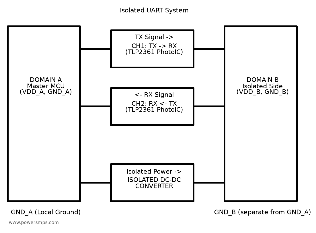
Building a bidirectional isolated UART link requires 2 independent channels to isolate transmit (TX→RX) and receive (RX←TX) paths respectively. The receivers on both sides demand valid power supplied independently within their respective ground domains. Typically, dedicated local rails or isolated DC-DC converters are placed alongside; because the signal isolators themselves do not transfer power, the receiver power subsystem must be planned separately.
Adopting digital isolators (such as the ISO7721 series) eliminates optical CTR degradation and aging mechanisms associated with LEDs; however, continuous quiescent power consumption and default output state under power loss must be scrutinized. For example, the TI ISO772x family is divided into standard versions that hold the output High when input power or signal is lost, and ‘F’ suffix versions that drive the output Low. Because UART sits at High during Idle, select a model whose default state matches system requirements. TI ISO772x Datasheet
Dielectric isolation capability should never be determined based solely on the short-term dielectric withstand voltage listed on the first page of a datasheet. Perform a thorough evaluation encompassing continuously applied working voltages, basic versus reinforced insulation requirements, creepage and clearance distances, PCB isolation barrier routing and isolation slots, and relevant safety standards. Near high-switching-noise environments such as inverters or power converters, select parts offering ample common-mode transient immunity (CMTI) margins compared to actual circuit \(dv/dt\) switching rates.
Board-level verification should be conducted systematically in the following phased sequence:
- Logic Polarity Verification: Verify that Idle High, start bit Low, and stop bit High logic polarities match precisely between transmitter TX and receiver RX.
- Dynamic Waveform and Pattern Testing: Transmit
0x55,0xAA,0x00,0xFF, and continuous long data frames while measuring edge transition times, PWD, receiver voltage levels, and communication frame errors. Pay close attention not only to continuous toggling but also to propagation delay on the first transition back to High after a prolonged Low (0x00) duration. - Temperature and Supply 4-Corner Testing: Test combinations of minimum and maximum target temperatures with minimum and maximum supply voltage rails. Confirm the impact on communication timing caused by drive current reduction from elevated LED forward voltage (\(V_F\)) at low temperatures, as well as CTR degradation and increased dark current at high temperatures.
- Power Interruption and Fault Disconnection Testing: Cycle transmitter and receiver power supplies independently, and simulate MCU reset and LED series signal line breaks. Verify that MCU error detection upon loss of communication, buffer flushing, and automatic re-establishment of communication following power restoration execute as designed.
9. Design Checklist
- Have you evaluated device propagation delay, PWD, and output voltage margins under your target baud rate and load conditions?
- Does the LED extinguish in the Idle High state, and is the signal properly transferred non-inverted from TX to RX?
- Have you calculated worst-case LED drive current accounting for GPIO output characteristics, resistor tolerances, temperature coefficients, and long-term aging margins?
- For high-temperature operation, have you directly verified the CTR-vs-temperature or fixed-IF IC-vs-temperature curve in the selected part datasheet?
- Have you clearly distinguished between typical curves versus guaranteed minimum ratings, and active-region CTR versus saturation-region CTR?
- Does the output pull-up resistance simultaneously satisfy both the static Low drive requirement (lower limit) and the dynamic rise-time specification (upper limit)?
- Have you examined the state of the RX line not only under normal receiver power, but also during MCU reset, open-line faults, and supply power-down conditions?
- Does the design satisfy isolated power and ground separation requirements across both domains, along with package and PCB creepage and clearance standards?