Non-isolated offline buck converters are widely used as auxiliary power supplies for smart meters, appliance control units, industrial sensors, and IoT devices. Power Integrations’ LinkSwitch-TN2 900V series (LNK3294, LNK3296) integrates a 900V-rated power MOSFET, oscillator, ON/OFF control logic, and a high-voltage bias current source onto a single IC, minimizing external component count while delivering high reliability in harsh power grid environments.
To reduce standby power below 30mW, an external bias design based on the EcoSmart architecture is essential. In addition, precisely calculating the FEEDBACK (FB) pin ON/OFF control resistor for the newer 2.0V reference voltage and securing 900V high-voltage safety clearances are required to ensure stable operation of the LNK3294 and LNK3296.
Table of Contents
- 1. Overview, LNK3294 vs. LNK3296 Specification Comparison, and Device Selection Criteria
- 2. EcoSmart Standby Power Reduction Mechanism: Self-Biasing vs. External Bias Design
- 3. FEEDBACK (FB) Pin ON/OFF Control Mechanism and Precision Resistor Design
- 4. Standby Mode Implementation Comparison: FB Pin Control vs. Output Load Disconnection (Load Switch)
- 5. Non-Isolated Buck Key Power Component Selection Guide: Diode, Inductor, and Bypass Capacitor
- 6. High-Voltage Safety Standards and PCB Layout: 900V Clearance Distances and Galvanic Isolation Interfaces
1. Overview, LNK3294 vs. LNK3296 Specification Comparison, and Device Selection Criteria
The LinkSwitch-TN2 900V family supports non-isolated buck, buck-boost, and isolated/non-isolated flyback topologies, and features an integrated 900V \(BV_{\text{DSS}}\) rated MOSFET. For industrial inputs exceeding the 85~265 VAC universal input range, suitability should not be evaluated solely by the 900V rating; steady-state DRAIN voltage, surge, clamp, and thermal conditions of the operating circuit must also be verified. Although the LNK3294 and LNK3296 share identical control architectures and pinouts, clear differences in class exist in internal MOSFET die size, on-resistance (\(R_{\text{DS(on)}}\)), peak current limit (\(I_{\text{LIMIT}}\)), and maximum output current capability.
| Parameter | LNK3294 | LNK3296 | Design Notes |
|---|---|---|---|
| MOSFET Breakdown Voltage (\(BV_{\text{DSS}}\)) | 900 V | 900 V | Identical voltage rating platform |
| Internal MOSFET \(R_{\text{DS(on)}}\) (100°C) | Approx. 31.0 Ω | Approx. 9.70 Ω | Conduction loss reduced by larger die size |
| Peak Current Limit (\(I_{\text{LIMIT(typ)}}\)) | 257 mA (Min. 240 mA / Max. 275 mA) | 482 mA (Min. 450 mA / Max. 515 mA) | LNK3296 delivers approx. 1.9x higher peak current |
| Maximum Output Current (Buck, MDCM) | Up to 120 mA | Up to 225 mA | Mostly discontinuous conduction mode |
| Maximum Output Current (Buck, CCM) | Up to 170 mA | Up to 360 mA | Continuous conduction mode |
| Available Package Options | PDIP-8C (P), SMD-8C (G) | PDIP-8C (P), SMD-8C (G) | Per official datasheet |
| Recommended Target Load Range | MCU boards, sensor nodes (~1~2W class) | Relay driving, Wi-Fi communication modules (3~5W+ class) |
According to the manufacturer’s official datasheet 900V output current table and ordering information, the LNK3294 and LNK3296 are available in PDIP-8C (P) and SMD-8C (G). Because SO-8C (D) is exclusive to the 725V family, designs must not assume LNK3294D or LNK3296D. Regardless of package selection, sufficient copper area must be provided for the SOURCE pins, and junction temperatures must be verified under actual input, load, and ambient temperature conditions.
2. EcoSmart Standby Power Reduction Mechanism: Self-Biasing vs. External Bias Design
LinkSwitch-TN2 employs a simple ON/OFF control scheme that enables or disables switching cycles based on the load. The standby supply current specified by the manufacturer is less than 100 µA. However, the overall no-load standby power of the converter differs significantly depending on the bias supply architecture.
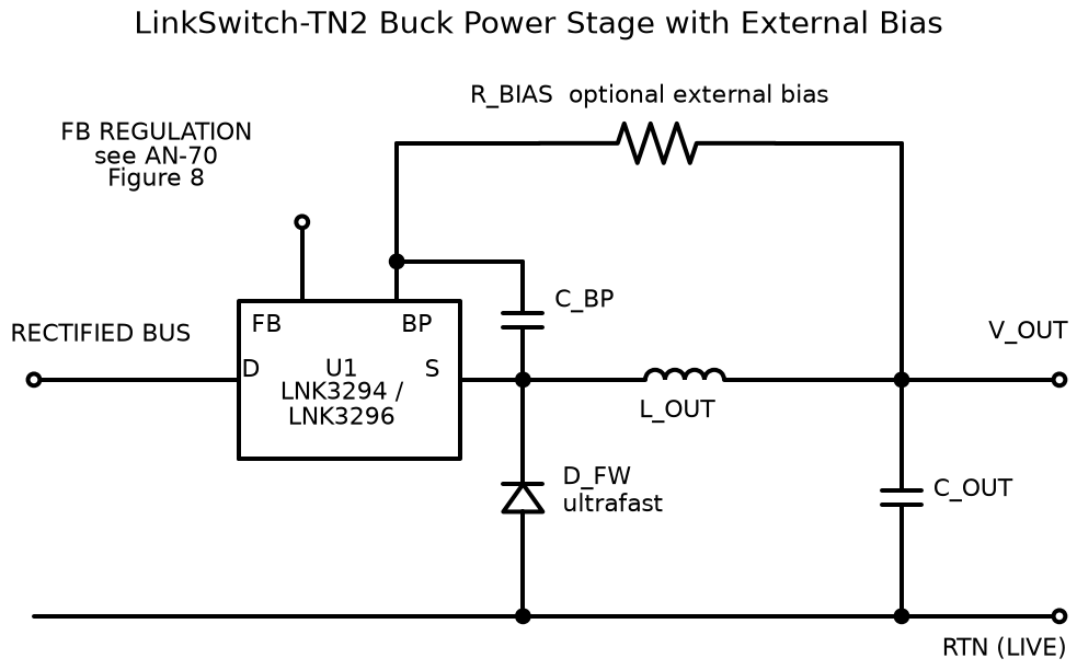
2.1 Self-Biasing Operation and Loss Factors
In self-biasing mode, without external bias components (\(D_{\text{BIAS}}\), \(R_{\text{BIAS}}\)), the internal high-voltage current source connected to the DRAIN pin continuously charges the BYPASS (BP) pin capacitor (\(C_{\text{BP}}\)). Because the high-voltage rectified bus voltage (\(V_{\text{IN(DC)}}\)) is applied directly across the internal current source, continuous current draw across a several-hundred-volt drop results in standby losses on the order of 50 ~ 100 mW.
2.2 Achieving Sub-30mW Standby Power via External Bias Configuration
To minimize no-load standby power, from the output (\(V_{\text{OUT}}\)) or an auxiliary winding, a fast diode (\(D_{\text{BIAS}}\)) and a current-limiting resistor (\(R_{\text{BIAS}}\)) must be connected to inject bias current into the BP pin. When external current flows into the BP pin and maintains the operating voltage of the internal bias regulator, the internal high-voltage current source automatically shuts off. Consequently, direct leakage and drop losses from the high-voltage line are eliminated, significantly reducing no-load standby power to below 30 mW.
The key to reducing standby power is disabling the internal high-voltage charging path using an external bias. Because actual no-load power consumption varies depending on input voltage and external component leakage currents, it must be verified on the finished product.
3. FEEDBACK (FB) Pin ON/OFF Control Mechanism and Precision Resistor Design
The FEEDBACK (FB) pin of the LinkSwitch-TN2 is not a conventional PWM voltage feedback node, but rather a current-sensing input that determines cycle-by-cycle switching decisions.
3.1 FB Pin Control Thresholds and Operating Mechanism
The current flowing into the FB pin (\(I_{\text{FB}}\)) is sampled at the beginning of each internal oscillator cycle.
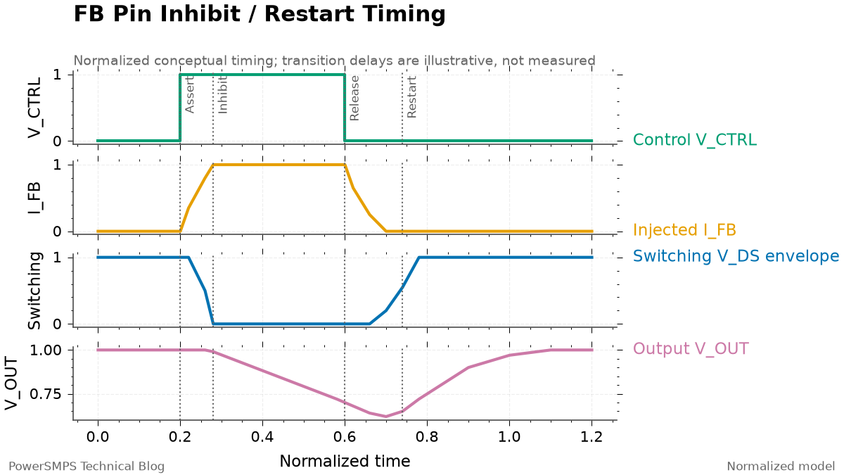
- Switching Inhibit Threshold (\(I_{\text{FB}}\)): When the current flowing into the FB pin exceeds a typical value of 49 µA, the internal comparator triggers to inhibit the MOSFET turn-on for that switching cycle.
- Line Overvoltage Shutdown Threshold (\(I_{\text{FBSD}}\)): If the FB pin input current exceeds \(I_{\text{FBSD}}\) (typical value of 670 µA) for 2 consecutive cycles, Line Overvoltage Protection (Line OVP) activates, completely halting switching and entering Auto-Restart mode.
Therefore, when injecting current into the FB pin via an external signal to forcefully disable switching, an adequate margin must be maintained so that the current is sufficiently above the switching inhibit threshold (49 µA) yet does not reach the overvoltage shutdown threshold (670 µA). The recommended control current range is 150 µA to 300 µA, with a design nominal value of approximately 200 µA.
3.2 Newer 2.0V Reference Voltage: Control Resistor (\(R_{\text{ctrl}}\)) Calculation
Care must be taken when dimensioning the control resistor not to adopt legacy LinkSwitch-TN parameters. The nominal FEEDBACK (FB) pin voltage (\(V_{\text{FB}}\)) of the newer LinkSwitch-TN2 is 2.0V (±1.25%). Applying the legacy LinkSwitch-TN value of 1.65V introduces calculation errors that risk deviating from the target injection current (200 µA).
When the external control supply voltage is \(V_{\text{ctrl}}\), the correct calculation formula for control resistor \(R_{\text{ctrl}}\) is as follows:
\[R_{\text{ctrl}} \approx \frac{V_{\text{ctrl}} – 2.0\,\text{V}}{200\,\mu\text{A}}\]For example, when \(V_{\text{ctrl}} = 5.0\,\text{V}\), \(R_{\text{ctrl}} \approx (5.0 – 2.0) / 200 \times 10^{-6} = 15\,\text{k}\Omega\) is obtained. If a 3.3V control supply is used, \(R_{\text{ctrl}} \approx (3.3 – 2.0) / 200 \times 10^{-6} = 6.5\,\text{k}\Omega\) (standard value of 6.2 kΩ or 6.8 kΩ) is applied.
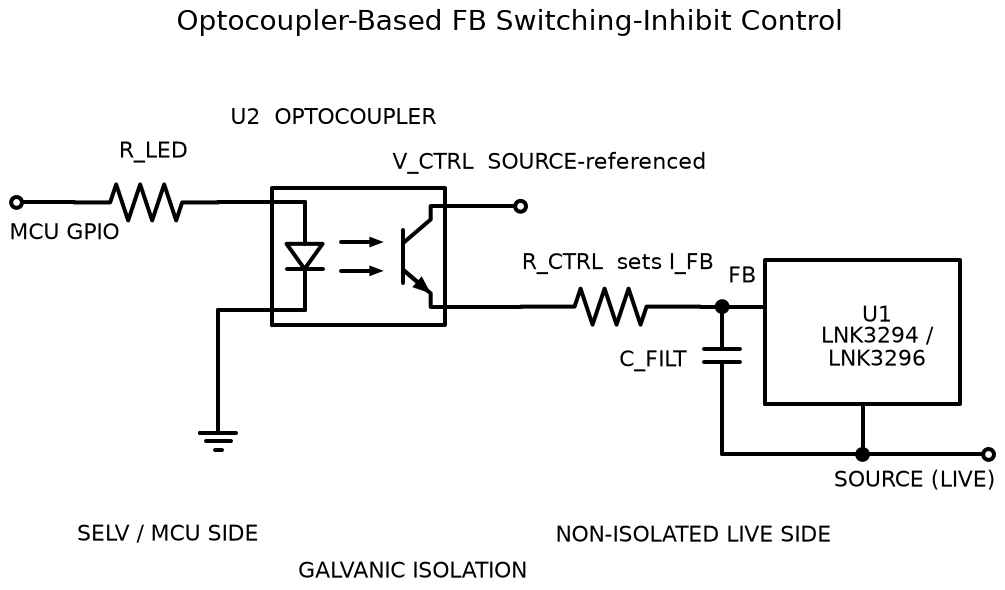
Because the FB pin is a high-impedance node, it must be physically separated from switching nodes (DRAIN, inductor, freewheeling diode), and if necessary, a ceramic capacitor (\(C_{\text{FILT}}\)) of several tens of picofarads should be placed in parallel between the FB and SOURCE pins to prevent high-frequency switching noise coupling.
4. Standby Mode Implementation Comparison: FB Pin Control vs. Output Load Disconnection (Load Switch)
Methods for reducing power consumption when a system enters standby mode are broadly divided into the FB pin forced pull-up method and the output load switch (P-MOSFET) disconnection method.
| Comparison Item | 1. Forced FB Pin Pull-Up Control (Switching Inhibit) | 2. Output Load Disconnection (P-MOSFET / Load Switch) | Design Considerations |
|---|---|---|---|
| Controlled Target | Inhibits IC internal MOSFET switching | Physically disconnects the output power supply path | |
| No-Load Standby Power | Excellent (sub-tens of mW) | Relatively high (tens to hundreds of mW) | FB control cuts off inductor/switching losses |
| Switching EMI and Ripple | Completely eliminated (switching stopped) | Residual (converter continues pulse skipping) | Advantageous during precision sensor measurement intervals |
| Control Switch Component Rating | Signal level (µA-class small TR or optocoupler) | Power level (must handle rated load and inrush current) | Reduces BOM cost and board area |
| Conduction Loss (IR Drop) | None | Voltage drop occurs due to series \(R_{\text{DS(on)}}\) | Affects efficiency at high load currents |
| Recovery Speed (Turn-on) | Requires restart and output capacitor charging time | Relatively fast (if output is already charged) | Consider system start-up time requirements |
In single-load systems where minimizing standby mode losses is paramount, the FB pin control approach—achievable with compact signal-level components—offers distinct advantages in BOM cost, mounting area, and thermal dissipation. Conversely, in environments such as communication modules where fast power recovery is required and output voltage must be maintained, adopting the output load switch method is more suitable.
5. Non-Isolated Buck Key Power Component Selection Guide: Diode, Inductor, and Bypass Capacitor
Because the high-voltage AC input connects directly to the inductor and switching device in a non-isolated buck converter, electrical ratings and limits of key power components must be strictly observed.
5.1 Freewheeling Diode (\(D_{\text{FW}}\)): Mandatory Ultrafast Diode Application
The freewheeling diode (\(D_{\text{FW}}\)), which sustains inductor current when the switching element turns off, must be an ultrafast recovery diode with a reverse recovery time (\(t_{\text{rr}}\)) of 75 ns or less, with a recommended specification of \(t_{\text{rr}} \le 35\,\text{ns}\). Because general-purpose standard rectifier diodes (such as 1N4007) exhibit reverse recovery times in the range of several microseconds, severe shoot-through current (reverse recovery current surge) flows from the high-voltage DC rail into the internal switch the instant the MOSFET turns on, causing immediate IC failure. Consequently, the use of general-purpose rectifier diodes such as 1N4007 is strictly prohibited.
5.2 Output Inductor (\(L_{\text{OUT}}\)): Securing Core Saturation Current (\(I_{\text{sat}}\)) Margin
If the inductor core saturates, inductance drops sharply, potentially causing excessive current to flow into the MOSFET. Therefore, the saturation current (\(I_{\text{sat}}\)) rating of the inductor must be equal to or greater than the maximum peak current limit (\(I_{\text{LIMIT(MAX)}}\)) of the LinkSwitch-TN2.
- LNK3294: Since \(I_{\text{LIMIT(MAX)}} = 275\,\text{mA}\), ensure a margin of at least \(I_{\text{sat}} \ge 300\,\text{mA}\).
- LNK3296: Since \(I_{\text{LIMIT(MAX)}} = 515\,\text{mA}\), ensure a margin of at least \(I_{\text{sat}} \ge 600\,\text{mA}\).
5.3 BYPASS Capacitor (\(C_{\text{BP}}\)) Mounting Requirements
A low-ESR ceramic capacitor (X7R or X5R dielectric) with a capacitance of 0.1 µF or 1.0 µF should be mounted at the BYPASS (BP) pin. Because this capacitor determines the bias supply stability of the internal control circuitry, it must be mounted immediately adjacent to the BP and SOURCE pins with minimal trace length to minimize parasitic inductance.
6. High-Voltage Safety Standards and PCB Layout: 900V Clearance Distances and Galvanic Isolation Interfaces
6.1 Output GND Potential and Galvanic Isolation in Non-Isolated Bucks
In a non-isolated buck topology, the output GND is directly connected to the negative (-) terminal of the rectified AC input bus. Because the output terminals are not referenced to protective earth (PE) and float at high-voltage AC line potentials, galvanic isolation devices such as optocouplers must be implemented when interfacing control signals with external system interfaces or host microcontrollers (MCUs) to prevent electrical shock hazards and controller damage.
6.2 900V High-Voltage Clearance Distances and PCB Layout Rules
To comply with safety standards and ensure reliable operation, apply the following layout guidelines.
- DRAIN Pin Isolation Distance: Apply a clearance of at least 2 mm around the DRAIN pin as an initial layout baseline. However, final creepage and clearance distances must be recalculated based on applicable safety standards, operating voltages, material groups, pollution degrees, overvoltage categories, and altitude conditions. If necessary, consider milling air slots between adjacent conductors.
- Primary Thermal Path: Allocate a large copper pour to traces connected to the SOURCE pins to lower thermal resistance.
- High-Frequency Current Loop Minimization: Minimize the loop area of the high-frequency switching loop (\(\text{high-d}i/\text{d}t\) loop)—formed by the input capacitor, MOSFET DRAIN-SOURCE, and freewheeling diode—to suppress radiated EMI.
Official Reference Documentation: Power Integrations LinkSwitch-TN2 Family Data Sheet, Rev. Q (June 2023). Orderable component packages, current limits, output currents, and FB pin thresholds should be cross-checked against the latest revision during actual design.