Tag: Relay Driver

  • 3.3V MCU Relay Driver MOSFET Selection: On-Resistance, Gate Resistor, and Voltage Rating Calculations

    3.3V MCU Relay Driver MOSFET Selection: On-Resistance, Gate Resistor, and Voltage Rating Calculations

    When using a 3.3V GPIO to control a 12V relay, you must first check the guaranteed on-resistance at the actual gate voltage rather than the MOSFET threshold voltage. Calculating the load current determined by power supply and coil tolerances, the drain peak voltage during coil turn-off, and the GPIO charge and discharge currents provides a clear rationale for component selection.

    The following is a low-speed DC relay ON/OFF design example based on assumed operating conditions, not empirical measurements from a specific product.

    1. Check Guaranteed On-Resistance Instead of VGS(th)

    In the AO3400A datasheet Rev 3.1, the threshold voltage VGS(th) is defined under the conditions of drain current 250µA and VDS=VGS. The minimum, typical, and maximum values are 0.65V, 1.05V, and 1.45V, respectively. This test current is a conduction current used to define the threshold, not a condition that guarantees low on-resistance at relay load currents.

    The manufacturer’s maximum on-resistance specifications are as follows. The junction temperature condition for the table is TJ=25°C.

    Gate Voltage VGS Test Drain Current Maximum RDS(on)
    2.5V 3A 48mΩ
    4.5V 5A 32mΩ
    10V 5.7A 26.5mΩ

    Even when using a 3.3V MCU, the GPIO High output is not always 3.3V. You must check the minimum VOH and load conditions in the MCU datasheet, and verify that VGS—accounting for voltage drops across the gate resistor network and source voltage fluctuations—is sufficiently higher than the test voltage specified in the on-resistance rating. Furthermore, the test currents in the on-resistance table must not be interpreted as allowable continuous currents on an actual PCB.

    Source: AO3400A Official Datasheet, electrical characteristics and thermal characteristics tables.

    2. Coil Current and Conduction Loss Calculations

    The example conditions are assumed as follows. The GPIO values are not guaranteed specifications of any specific MCU.

    Item Example Assumption
    Nominal coil voltage and resistance 12V·120Ω
    Maximum supply voltage 13.2V
    Minimum coil resistance considering low temperature and tolerance 108Ω
    Minimum GPIO VOH 2.9V
    Gate charging current budget 4mA
    On-resistance used for calculation 48mΩ, VGS=2.5V·TJ=25°C specification

    The nominal current is 12V/120Ω=100mA, and the assumed maximum current is as follows:

    \[I_{coil,max}=\frac{13.2}{108}\approx0.12222\ \mathrm{A}\]

    Conduction loss is proportional to the square of current:

    \[P_{cond}=I_{coil}^{2}R_{DS(on)}\]

    The calculated value at nominal current is 0.100²×0.048=0.00048W, or 0.48mW. Under the assumed maximum current condition, it is approximately 0.12222²×0.048=0.000717W, or 0.717mW.

    This value is a conduction loss calculation applying the 25°C on-resistance. It is not a final guaranteed temperature value that includes on-resistance increases at high temperatures, switching losses, and actual PCB heat dissipation conditions. Because datasheet thermal characteristics are based on a 2oz copper, 1in² FR4 board in still air, actual board conditions must be verified separately.
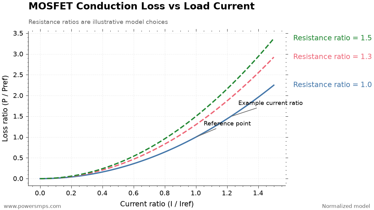
    Normalized conduction loss according to current ratio and on-resistance ratio. Resistance multipliers 1.0, 1.3, and 1.5 are assumptions for comparison and not guaranteed values at specific temperatures.
    Normalized conduction loss according to current ratio and on-resistance ratio. Resistance multipliers 1.0, 1.3, and 1.5 are assumptions for comparison and not guaranteed values at specific temperatures.

    The resistance multipliers 1.0, 1.3, and 1.5 in the graph are model values chosen for comparison. They are not manufacturer-guaranteed values or measured data corresponding to specific temperatures. Under the same on-resistance, the graph shows the relationship where conduction loss increases by a factor of 1.44 when the current increases by a factor of 1.2.

    3. GPIO, Gate, and Relay Interconnection Conditions
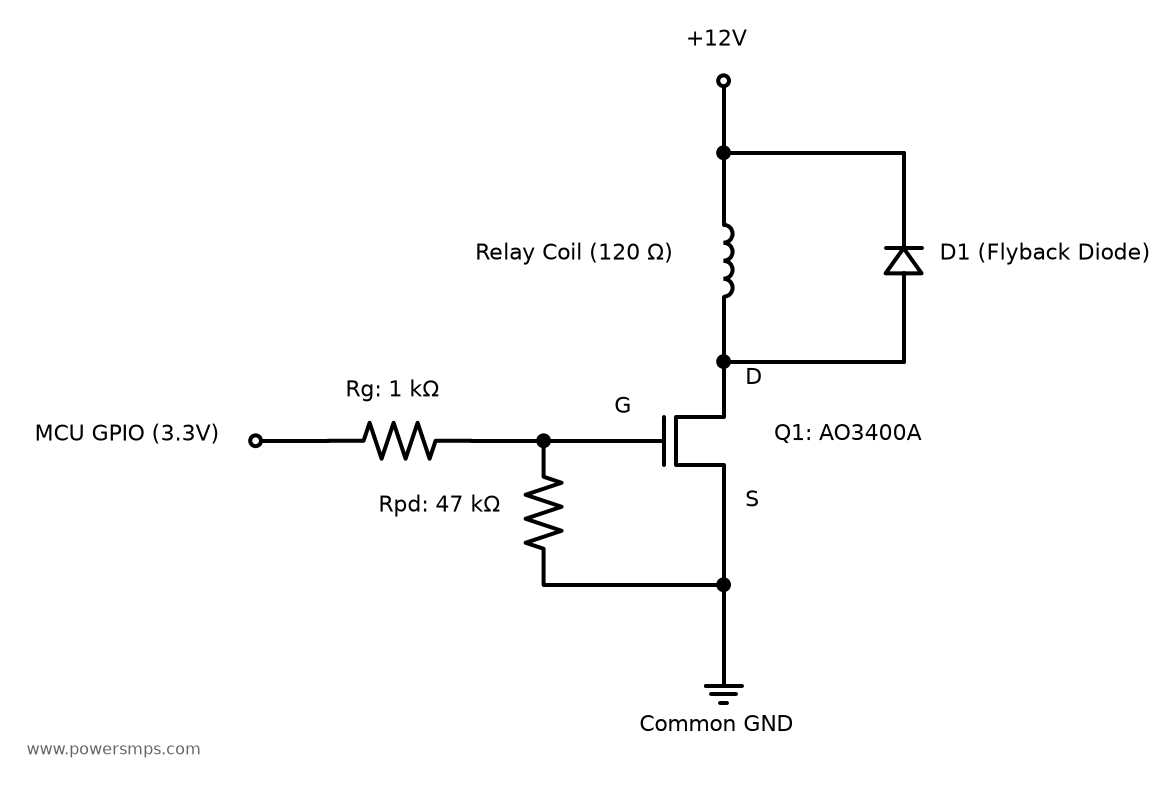
    3.3V GPIO, 1kΩ gate resistor, 47kΩ pull-down, and AO3400A MOSFET circuit driving a 12V relay. A flyback diode is connected across the coil, and ground is shared.
    Low-side drive example for a 12V·120Ω relay coil. The cathode of the flyback diode is connected to +12V. Review component values together with the selection criteria in the main text.

    The example is a low-side N-MOSFET circuit where the MCU and load supply share a common ground. Connections are listed in the following table:

    Device / Node Connection
    Relay coil Between +12V and Q1 drain
    Q1 source Common GND shared with MCU
    Series gate resistor Rg Between GPIO and Q1 gate, example value 1kΩ
    Pull-down resistor Rpd Between Q1 gate (downstream of Rg) and source, example value 47kΩ
    Flyback diode D1 Cathode to +12V, anode to Q1 drain

    The body diode of a low-side N-MOSFET conducts from source to drain. When the coil is turned off and the drain flies up to a positive voltage higher than the supply, the body diode is reverse-biased and cannot substitute for the coil flyback freewheeling path.

    The relationship between diode ratings and relay release time can be further referenced in the previous article, Relay Flyback Diode Selection and Turn-Off Time Calculations.

    4. Series Gate Resistor and Pull-Down Calculations

    Modeling the GPIO as an ideal 3.3V voltage source and budgeting an initial gate charging current of 4mA, the lower limit calculation for the external series resistance is 3.3V/4mA=825Ω. In the example, 1kΩ is selected. Neglecting the GPIO internal output resistance, the calculated initial current upper limit is 3.3V/1kΩ=3.3mA. For actual component selection, verify both recommended source/sink currents and VOH/VOL conditions in the MCU datasheet. Never use the absolute maximum rated current as a continuous driving target.

    Connecting a 47kΩ pull-down behind the gate creates voltage division in steady state. Under the conditions of minimum VOH 2.9V, negligible gate leakage, and a common ground without source voltage bounce, the calculation is as follows:

    \[V_{GS}=2.9\times\frac{47}{1+47}\approx2.8396\ \mathrm{V}\]

    Under this DC assumption, the voltage is higher than the test voltage for the 2.5V on-resistance specification. In practical circuits, verify margin across temperature, supply tolerances, and source voltage variations. When the GPIO outputs 3.3V, the DC current flowing through the resistor network is 3.3V/48kΩ=68.75µA.

    A static calculation is also possible for when the GPIO is High-Z during reset. Assuming a total leakage current of 1µA and an allowable gate voltage of 0.3V, Rpd≤0.3V/1µA=300kΩ. With 47kΩ, the static leakage voltage is approximately 47mV. While the pull-down should be placed close to the gate, this calculation does not guarantee prevention of false turn-on caused by Miller current injection during rapid drain voltage changes or across all power sequencing conditions.

    5. MOSFET Voltage Rating Calculations with Coil Clamping

    The absolute maximum VDS rating of the AO3400A is 30V. When selecting a device, adequate design margin must exist for the following voltage sum:

    \[V_{sup,max}+V_{clamp,max}+V_{overshoot} < V_{DS,rating}\]

    Assuming a clamp voltage of 1V for a standard diode and a wiring overshoot of 3V, the peak is 13.2+1+3=17.2V. Although this is lower than 30V, this confirms only the assumed voltage sum, so actual drain waveforms and component tolerances must be verified.

    Conversely, in an assumption combining a 24V Zener and a 0.8V forward-voltage diode, even without overshoot the sum is 13.2+24+0.8=38V. Therefore, the 30V AO3400A cannot be used under these conditions. When selecting higher voltage-rated devices, evaluate based on the Zener’s actual clamp current, temperature, tolerance, and wiring surges. Sizing MOSFET voltage rating based solely on supply voltage makes it easy to overlook this difference.

    6. Distinguishing and Validating Low-Speed ON/OFF vs. PWM

    The total gate charge Qg of the AO3400A is typical 6nC and maximum 7nC, but the test conditions are VGS=4.5V, VDS=15V, and ID=5.7A. This must not be used as a guaranteed charge value under 3.3V drive. Furthermore, Qg/Ig is a coarse charging time estimate and does not equal the actual drain transition time including the Miller plateau. For relevant principles, refer to the TI SLUA618A Gate Driver Design Document.

    Do not apply resistor values for low-speed relay ON/OFF directly to high-speed PWM solenoid circuits. Whether a dedicated driver is required should be determined by examining gate charge, GPIO source/sink capability, switching losses, temperature, and the EMI budget together.

    The final verification sequence is as follows:

    1. Recalculate maximum current using actual component coil tolerances and supply voltage ranges.
    2. Measure gate-to-source voltage during normal operation to verify it meets the on-resistance guarantee condition.
    3. Check for spurious gate turn-on and source voltage bounce during boot, reset, and power-up sequencing.
    4. Verify that the drain peak and ringing during coil turn-off remain within the selected breakdown voltage margin.
    5. Check heat dissipation on the actual PCB and at operating temperatures.

    The core sequence is Verify guaranteed on-resistance at actual VGS → Calculate maximum coil current and losses → Validate gate resistor network → Verify VDS including clamp. The 1kΩ and 47kΩ in this example are a starting point calculated under these conditions, and must be reconfirmed against the datasheets of the MCU and relay to be used.
  • Relay Flyback Diode Selection: Sizing by Coil Current and Release Time

    Relay Flyback Diode Selection: Sizing by Coil Current and Release Time

    Relay Coil Driving and Counter-EMF Suppression Design Challenges

    Electromechanical relays are critical components that provide complete galvanic isolation between control circuits and high-power loads. However, the relay coil—the mechanical actuation mechanism—is a typical inductive load that induces a high voltage spike, known as inductive kickback, when current is interrupted.

    When the current flowing through the coil is abruptly interrupted, the counter-electromotive force (counter-EMF) generated by the inductance \(L\) is governed by Faraday’s law:

    \[v_L(t) = -L \frac{di}{dt}\]

    During the brief switching transition (tens to hundreds of ns) when the low-side transistor (MOSFET or BJT) turns off, \(\frac{di}{dt}\) takes on a very large negative value, creating a positive high-voltage spike of several hundred volts or more at the drain (or collector) node of the switching device. Without an adequate surge suppression circuit, this spike exceeds the breakdown voltage (\(V_{(BR)DSS}\)) of the switching device, causing permanent damage.

    The most common countermeasure is placing a single flyback diode (freewheeling diode) in anti-parallel across the coil. However, while a simple diode clamping circuit protects the drive transistor, it introduces a secondary (2nd) trade-off: it significantly delays the relay release time, leading to contact erosion and contact welding.

    Fundamental concepts of counter-EMF suppression for inductive loads have also been covered in the guides on SMPS gate driver inductive counter-EMF suppression techniques and low-side MOSFET switch selection and snubber design. This article outlines quantitative calculation methods and engineering decision criteria to size optimal flyback and clamping diodes based on relay coil current (\(I_{coil}\)) and required release time.


    Basic Parameter Selection: Sizing Coil Current (\(I_F\)) and Reverse Breakdown Voltage (\(V_{RRM}\))

    The primary (1st) electrical parameters that must be satisfied when selecting a single flyback diode are the forward current rating (\(I_F\)) and repetitive peak reverse voltage (\(V_{RRM}\)).

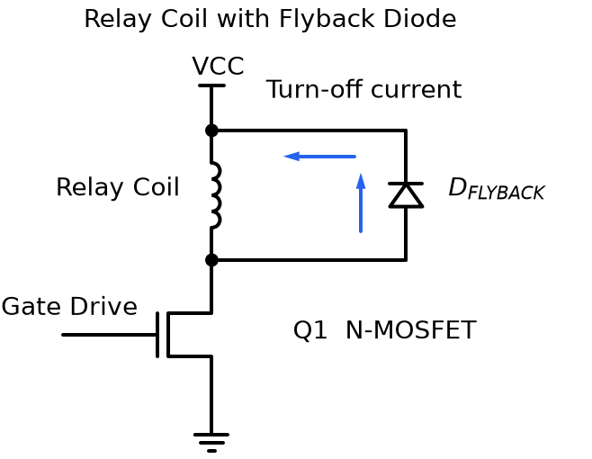
    Basic driver circuit schematic comprising a relay coil, low-side N-MOSFET switch, and parallel single flyback diode, showing the forward commutation current loop at turn-off
    Basic driver circuit schematic comprising a relay coil, low-side N-MOSFET switch, and parallel single flyback diode, showing the forward commutation current loop at turn-off

    1. Coil Steady-State Current (\(I_{coil}\)) and Diode Forward Rating (\(I_F, I_{FSM}\))

    When the relay is fully picked up in the ON state, the DC steady-state current \(I_{coil}\) flowing through the coil is determined by Ohm’s law from the applied coil voltage \(V_{coil}\) and the coil DC resistance \(R_{coil}\):

    \[I_{coil} = \frac{V_{coil}}{R_{coil}}\]

    The instant the switching device turns off, magnetic flux and current continuity in the inductor dictate that the entirety of \(I_{coil}\) flowing through the coil immediately commutates into the forward path of the flyback diode. Therefore, the initial peak forward current \(I_{F(peak)}\) applied when the diode turns on matches the steady-state coil current:

    \[I_{F(peak)} = I_{coil}\]
    • Average Forward Current Rating (\(I_{F(AV)}\)): In general control applications where the relay coil switching frequency is a few Hz or less, the continuous forward rating \(I_{F(AV)}\) of the diode must be equal to or greater than \(I_{coil}\) to prevent thermal breakdown.
    • Non-Repetitive Peak Surge Current (\(I_{FSM}\)): To withstand the transient peak current \(I_{F(peak)}\) immediately after turn-off, the diode’s \(I_{FSM}\) rating must sufficiently exceed \(I_{coil}\). General-purpose devices such as the 1N400x series (\(I_{F(AV)} = 1\text{A}, I_{FSM} = 30\text{A}\)) or 1N4148 (\(I_{F(AV)} = 150\sim 200\text{mA}, I_{FSM} = 1\sim 4\text{A}\)) easily satisfy the forward current requirements of typical small to medium control relays (\(I_{coil} \approx 20\text{mA} \sim 150\text{mA}\)).

    2. Diode Reverse Voltage (\(V_{RRM}\)) Margin Sizing

    When the switching device is ON, the supply voltage \(V_{CC}\) is applied in the reverse direction across the diode. Under ideal steady-state conditions, operation is possible as long as the diode reverse breakdown voltage \(V_{RRM}\) is greater than \(V_{CC}\); however, real power rails experience superimposed switching noise, parasitic wiring inductance, and power-up surges.

    Manufacturer technical guidelines (Panasonic Relay Technical Guide, Omron General-purpose Relay Precautions) specify the following \(V_{RRM}\) margin criteria:

    • General Industrial/Consumer DC Supplies (\(12\text{V}, 24\text{V}\)): To account for supply transient voltage margins, a minimum of \(V_{RRM} \ge (2 \sim 3) \times V_{CC}\) must be secured. For example, in a \(24\text{V}\) supply system, a diode rated for \(V_{RRM} \ge 72\text{V}\) or higher is selected, and in practice, general-purpose rectifier diodes rated at \(400\text{V} \sim 1000\text{V}\) (1N4004~1N4007) are used to provide ample headroom.
    • Automotive and Harsh Environments: In automotive electrical environments where load dump events and high-energy line surges are frequent, a rating of \(V_{RRM} \ge 10 \times V_{CC}\) or higher must be selected, or a dedicated TVS diode must be placed in parallel at the supply stage.

    Caution (Not Applicable to AC Coil Relays): Flyback diodes are surge suppression devices dedicated exclusively to direct current (DC) coil relays. Connecting a diode in parallel across an AC coil relay driver circuit will short the power supply every half cycle and cannot be used; AC systems require an RC snubber (CR circuit) or an MOV (Metal Oxide Varistor)/varistor.


    Single Flyback Diode Trade-Offs: Release Time Delay and Contact Welding Risks

    If only the protection of the switching device is considered, the single diode method—which clamps the coil counter-EMF to the diode forward voltage (\(V_F \approx 0.7\text{V}\)) level—is the simplest and lowest-cost approach. However, this causes critical side effects on the reliability of the relay itself.

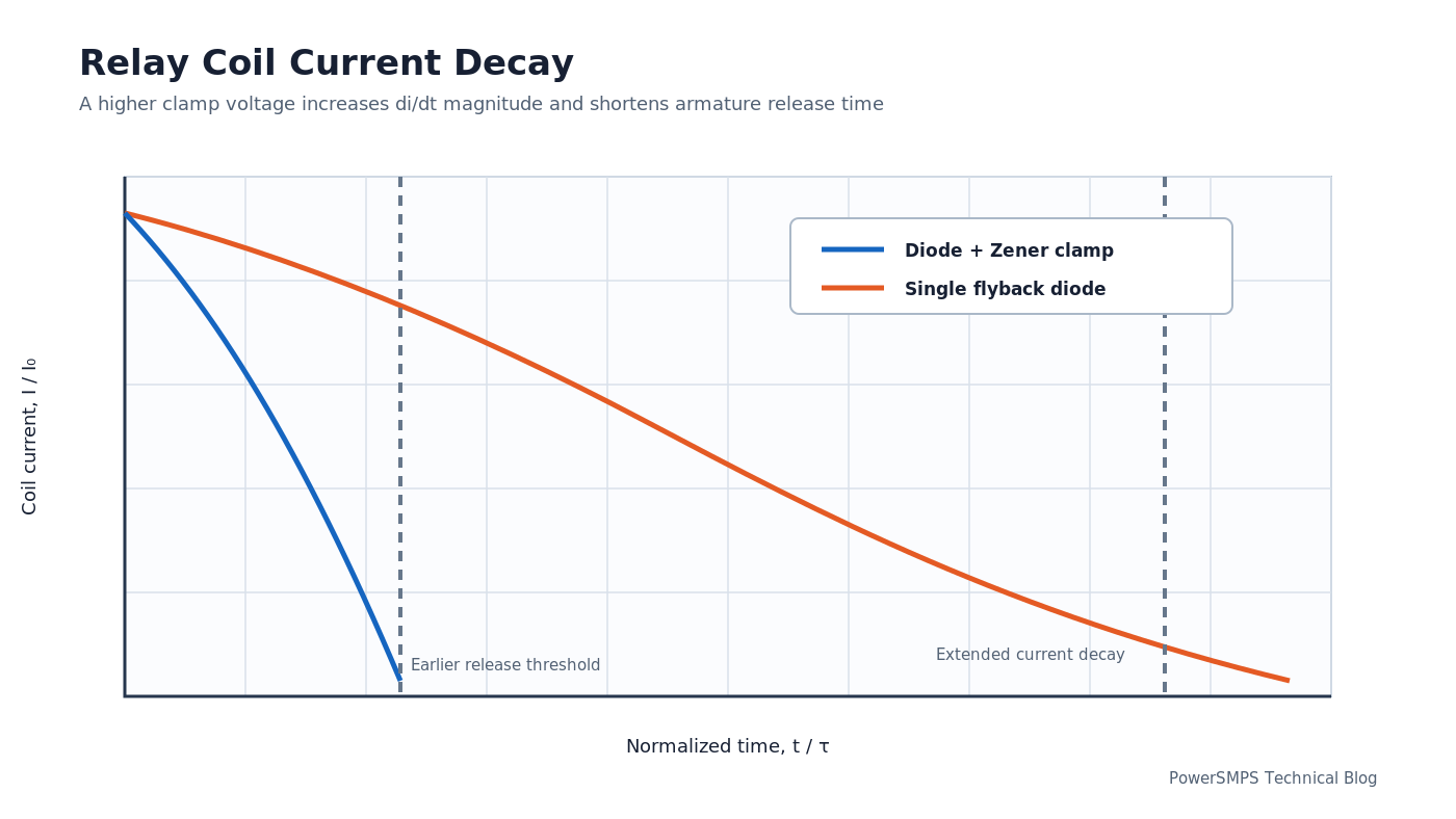
    Comparison waveforms of gradual exponential current decay (long time constant) with a single flyback diode versus rapid linear current decay and release time with a diode + Zener clamp
    Comparison waveforms of gradual exponential current decay (long time constant) with a single flyback diode versus rapid linear current decay and release time with a diode + Zener clamp

    1. Discharge Time Constant and Release Time (\(t_{release}\)) Delay Mechanism

    When the switch turns off, the magnetic energy stored in the coil is dissipated as it circulates through the closed loop formed by the coil internal resistance \(R_{coil}\) and the diode. The Kirchhoff’s Voltage Law (KVL) equation for this closed loop is as follows:

    \[L \frac{di(t)}{dt} + i(t) R_{coil} + V_F = 0 \Rightarrow \frac{di(t)}{dt} = -\frac{V_F + i(t) R_{coil}}{L}\]

    Because the forward voltage drop \(V_F\) of the diode is very low at approximately \(0.7\text{V}\), the counter-EMF voltage loop driving the inductor current toward 0 is extremely weak. The current decay progresses gradually and exponentially according to the inherent circuit time constant \(\tau = \frac{L}{R_{coil}}\).

    According to manufacturer measurement data, the relay opening/release time (Release Time) when using a single flyback diode is delayed by approximately 2 times to more than 5 times compared to the ideal open-circuit state without surge protection.

    2. Contact Arc Discharge and Contact Welding Mechanisms

    According to studies by leading relay manufacturers TE Connectivity (Application Note 13C3264) and Panasonic, this delay in coil current decay triggers the following contact failure chain reaction:

    1. Reduced Armature Travel Speed: As the coil current slowly decreases below the must-release voltage (Must Release Voltage / Drop-out Threshold), the magnetic pull of the coil releases the return spring force only gradually.
    2. Delayed Contact Separation Velocity: The initial opening velocity when the movable contact separates from the stationary contact slows down significantly.
    3. Extended Arc Duration: The plasma arc generated as the contact gap widens during load current interruption cannot be quenched rapidly and persists for an extended duration.
    4. Contact Erosion and Material Transfer: The high-temperature arc locally melts and spatters the contact metal (silver alloys, etc.).
    5. Occurrence of Contact Welding: Degraded contact surface roughness and micro-welding during re-solidification prevent the relay from returning, resulting in permanent welded-contact failure.

    Therefore, single flyback diode topologies should be avoided in circuits switching inrush or inductive loads, such as motors, solenoids, incandescent lamps, and large capacitor banks.


    Diode + Zener Clamp Design and Timing Calculations for Fast Release and Contact Protection

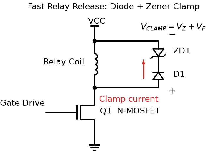
    The standard engineering solution to safely protect switching devices while preserving contact opening speed is connecting a standard diode and a Zener diode back-to-back (in series opposition).

    Fast surge suppression circuit schematic with a standard diode and Zener diode connected back-to-back (in series opposing) across the relay coil, showing clamping voltage polarities
    Fast surge suppression circuit schematic with a standard diode and Zener diode connected back-to-back (in series opposing) across the relay coil, showing clamping voltage polarities

    1. Discharge Voltage Clamping and Accelerated Current Decay Principle

    When the switching device turns off, the coil counter-EMF forces the Zener diode into its breakdown region. At this point, the clamping voltage \(V_{clamp}\) formed in the discharge loop is the sum of the Zener voltage \(V_Z\) and the diode forward voltage \(V_F\):

    \[V_{clamp} = V_Z + V_F\]

    The differential equation for the loop current decay is modified as follows:

    \[\frac{di(t)}{dt} = -\frac{V_Z + V_F + i(t) R_{coil}}{L}\]

    Because the Zener voltage \(V_Z\) is significantly larger than the coil internal voltage drop (\(i \cdot R_{coil}\)), the current decay slope \(\frac{di}{dt}\) forms a steep, nearly linear slope, discharging the current rapidly.

    2. Release Time (\(t_{release}\)) Calculation Formula

    The time \(t_{decay}\) required for the coil current to decay from steady-state current \(I_{coil}\) to the drop-out current \(I_{drop}\) where the relay armature begins to release is calculated via linear approximation as follows:

    \[t_{decay} \approx \frac{L \cdot (I_{coil} – I_{drop})}{V_Z + V_F}\]
    • \(L\): Coil inductance (\(\text{H}\))
    • \(I_{coil}\): Steady-state coil current (\(\text{A}\))
    • \(I_{drop}\): Relay release current threshold (\(\text{A}\), typically \(10\% \sim 30\%\) of rated current)
    • \(V_Z\): Zener diode breakdown voltage (\(\text{V}\))
    • \(V_F\): Forward voltage of the series standard diode (\(\text{V} \approx 0.7\text{V}\))

    As \(V_Z\) increases, the denominator grows larger, resulting in a dramatic reduction in the decay time \(t_{decay}\).

    3. Zener Voltage (\(V_Z\)) Sizing Criteria

    To restore contact separation velocity to unprotected levels and maximize contact lifespan, the Panasonic Application Guide recommends sizing the Zener voltage as follows:

    \[V_Z \ge 3 \times V_{coil}\]
    • \(12\text{V}\) relay coils: \(V_Z \ge 36\text{V}\) (select standard Zener ratings such as \(36\text{V}, 39\text{V}, 43\text{V}\))
    • \(24\text{V}\) relay coils: \(V_Z \ge 72\text{V}\) (select standard Zener ratings such as \(75\text{V}, 82\text{V}\))

    Drive Switch (MOSFET) Voltage Margin and Zener Pulse Power Rating Verification

    While applying a Zener diode to increase the discharge voltage improves relay contact reliability, it inversely increases the drain-to-source voltage (\(V_{DS}\)) stress that the low-side switching device must withstand. Therefore, quantitative verification of both the switch voltage rating and Zener power dissipation is essential.

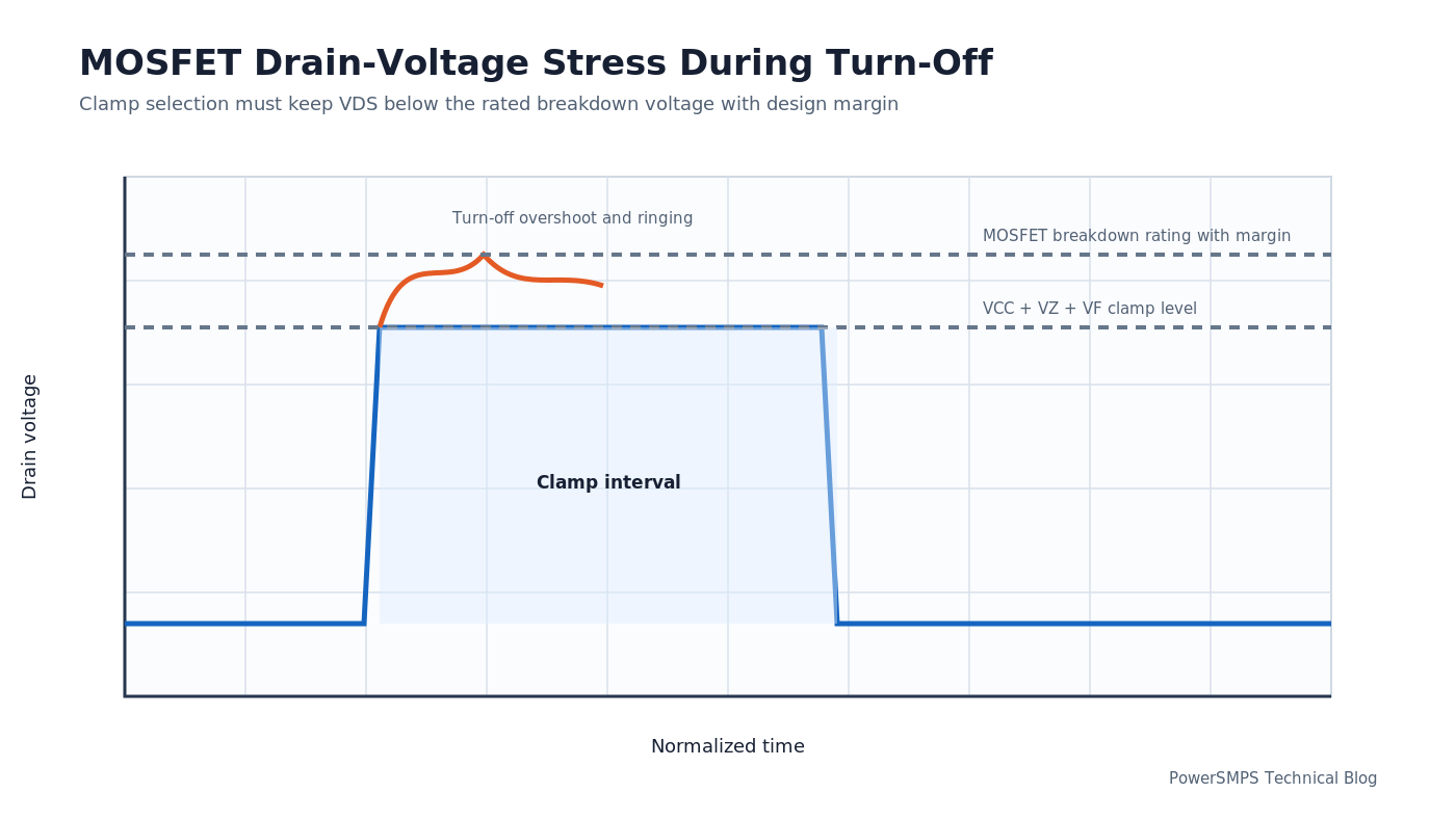
    Transient voltage waveform showing drain-to-source voltage (V_DS) clamped to V_CC + V_Z + V_F during low-side MOSFET turn-off and Safe Operating Area (SOA) margin indication
    Transient voltage waveform showing drain-to-source voltage (V_DS) clamped to V_CC + V_Z + V_F during low-side MOSFET turn-off and Safe Operating Area (SOA) margin indication

    1. Low-Side Switch Maximum Applied Voltage and Voltage Rating Margin

    At the instant of turn-off, the drain terminal voltage \(V_{DS(max)}\) of the low-side MOSFET is superimposed by the coil clamping voltage on top of the supply voltage \(V_{CC}\):

    \[V_{DS(max)} = V_{CC} + V_Z + V_F\]

    Accordingly, the breakdown voltage rating \(V_{(BR)DSS}\) of the MOSFET must be selected to include a safety margin of \(20\% \sim 30\%\) as follows:

    \[V_{(BR)DSS} \ge 1.25 \times (V_{CC} + V_Z + V_F)\]

    [Design Calculation Example]

    • Supply Voltage: \(V_{CC} = 24\text{V}\)
    • Coil Rating: \(V_{coil} = 24\text{V}, R_{coil} = 600\,\Omega \Rightarrow I_{coil} = 40\text{mA}\)
    • Zener Diode: \(V_Z = 75\text{V}\) (\(V_Z \approx 3.1 \times V_{coil}\))
    • Series Diode: \(V_F = 0.7\text{V}\)

    Peak voltage applied across the switch: \[V_{DS(max)} = 24\text{V} + 75\text{V} + 0.7\text{V} = 99.7\text{V}\]

    Required breakdown voltage with a \(1.25\) safety margin factor: \[V_{(BR)DSS} \ge 99.7\text{V} \times 1.25 \approx 124.6\text{V}\]

    Therefore, an N-channel MOSFET rated for \(150\text{V}\) or higher must be selected as the drive transistor to secure adequate Safe Operating Area (SOA) headroom. If the existing circuit switch rating is constrained to \(60\text{V}\) or \(100\text{V}\), trade-off adjustments are necessary, such as lowering \(V_Z\) (e.g., \(V_Z \approx 1 \sim 1.5 \times V_{coil}\)) or upgrading the switch to a higher-voltage device.

    2. Zener Diode Pulse Power and Energy Dissipation Verification

    The magnetic energy \(E\) stored in the coil inductance at turn-off is given by:

    \[E = \frac{1}{2} L I_{coil}^2\]

    Most of this energy is dissipated as heat in the Zener diode during the extremely brief discharge time (\(t_{decay}\)) immediately following switch turn-off.

    • Instantaneous Peak Pulse Power (\(P_{peak}\)): \[P_{peak} \approx V_Z \times I_{coil}\] In the example above, a peak power of \(P_{peak} \approx 75\text{V} \times 0.04\text{A} = 3.0\text{W}\) is applied. Verify that this provides sufficient margin compared to the non-repetitive peak pulse power (\(P_{PPM}\)) rating of the Zener diode (or unidirectional TVS diode) (typically \(400\text{W} \sim 600\text{W}\)).
    • Average Power Dissipation (\(P_{avg}\)): Where the switching operating frequency is \(f_{sw}\), the continuous power dissipation of the Zener is as follows: \[P_{avg} = E \times f_{sw} = \frac{1}{2} L I_{coil}^2 f_{sw}\] Under typical relay switching conditions (\(f_{sw} < 1\text{Hz}\)), the average power is less than a few mW; thus, standard SMD Zener diodes rated at \(500\text{mW} \sim 1\text{W}\) easily ensure thermal stability.

    Design Decision Summary: Relay Protection Circuit Topology Selection Guide

    The selection of a relay coil surge suppression circuit is a clear engineering trade-off between minimizing circuit cost and switch voltage stress versus preserving relay release speed and contact lifespan.

    1. Protection Circuit Topology Comparison Matrix

    Parameter / Feature Single Flyback Diode Diode + Zener Clamp Parallel Resistor / RC Snubber
    Discharge Loop Voltage (\(V_{clamp}\)) \(V_F \approx 0.7\text{V}\) (Extremely low voltage) \(V_Z + V_F\) (Designer configurable) \(I_{coil} R\) (Large initial voltage spike)
    Relay Release Delay (\(t_{release}\)) Very High (2~5x delay) Very Low (Restored to unprotected baseline) Moderate delay
    Contact Arc & Lifespan Impact Increased arc duration \(\rightarrow\) welding risk Rapid arc quenching \(\rightarrow\) contact lifespan preserved Moderate
    Switch Voltage Stress (\(V_{DS}\)) \(V_{CC} + 0.7\text{V}\) (Lowest stress) \(V_{CC} + V_Z + V_F\) (Higher switch voltage rating required) \(V_{CC} + I_{coil} R\)
    Component Count & Cost 1 diode (Lowest cost) 1 diode + 1 Zener (Moderate) Resistor / capacitor (Moderate)
    Recommended Applications Non-critical signal relays, light-load switching Power relays, inductive/inrush loads, high-reliability control AC relay coil control

    2. Practical Hardware Design Checklist

    1. Verify Steady-State Coil Current: After calculating \(I_{coil} = V_{coil} / R_{coil}\), confirm that the diode’s \(I_{F(AV)}\) and \(I_{FSM}\) are equal to or greater than \(I_{coil}\).
    2. Verify Reverse Voltage Margin: Ensure that \(V_{RRM}\) of the single diode or series diode meets at least \(V_{RRM} \ge 2\sim 3 \times V_{CC}\) (\(10 \times V_{CC}\) in harsh environments).
    3. Select Topology Based on Load Characteristics:
    4. When switching high-power or inductive loads such as motors, solenoids, heaters, or power rails, adopt the diode + Zener clamp topology as standard to preserve contact lifespan.
    5. Consider a single flyback diode only for simple indicators or low-power resistive loads where bill-of-materials (BOM) cost must be minimized aggressively.
    6. Align Zener Voltage and Switch Breakdown Margin:
    7. Set the Zener voltage to approximately \(V_Z \ge 3 \times V_{coil}\).
    8. Verify that the low-side MOSFET breakdown voltage satisfies \(V_{(BR)DSS} \ge 1.25 \times (V_{CC} + V_Z + V_F)\).
    9. Evaluate Zener Surge Pulse Power: Confirm that \(P_{peak} \approx V_Z \times I_{coil}\) is within the allowable non-repetitive peak pulse power rating of the Zener or TVS diode.