I once used a 74595-series shift register to expand limited MCU output ports. However, during testing where a 1 kV burst was applied to the AC power port in accordance with EN 55014-2, an issue occurred where the output data shifted by 1 bit.
Replacing the part with the TI SN74HCS595 featuring Schmitt-trigger inputs reduced the malfunction frequency, but the symptom persisted. While retaining the SN74HCS595, after adding an RC filter with a 100 Ω series resistor and a 1 nF capacitor to the CLK path, the phenomenon no longer occurred under the test conditions. This article summarizes the filter arrangement and troubleshooting process when distributing CLK to multiple ICs.
The 74595 architecture separates the shift register from the output storage register. In the case of the SN74HCS595, serial input data is shifted on the rising edge of SRCLK, and a separate RCLK updates the output storage register. This operational structure can be confirmed in the TI SN74HCS595 datasheet.
If an unintended CLK edge is falsely detected during shifting, the data can shift by an extra bit. When RCLK subsequently updates the outputs, the shifted data appears on the parallel outputs.
Based on the symptom of the output shifting by 1 bit and the improvement achieved after applying the CLK filter, we determined that this issue was caused by burst noise coupling into the shift CLK trace and being falsely recognized as additional clock pulses.
Switching to the SN74HCS595: Frequency Reduced, but Symptom Persisted
First, we replaced the IC with the TI SN74HCS595, which has Schmitt-trigger inputs. This device incorporates Schmitt-trigger architecture on all inputs, accommodating slow or noisy input signals. TI Datasheet
A Schmitt trigger uses different switching thresholds for rising and falling input voltages. This hysteresis reduces repeated switching caused by chatter near the input threshold. However, if noise swings across both switching thresholds, even a Schmitt-trigger input can register it as a clock pulse.
In practice, after replacing the IC, the malfunction frequency decreased, but the bit-shift issue did not disappear entirely. Because input hysteresis alone was insufficient in this environment, we added a countermeasure to attenuate the noise reaching the CLK input.
Adding a 100 Ω and 1 nF RC Filter to CLK
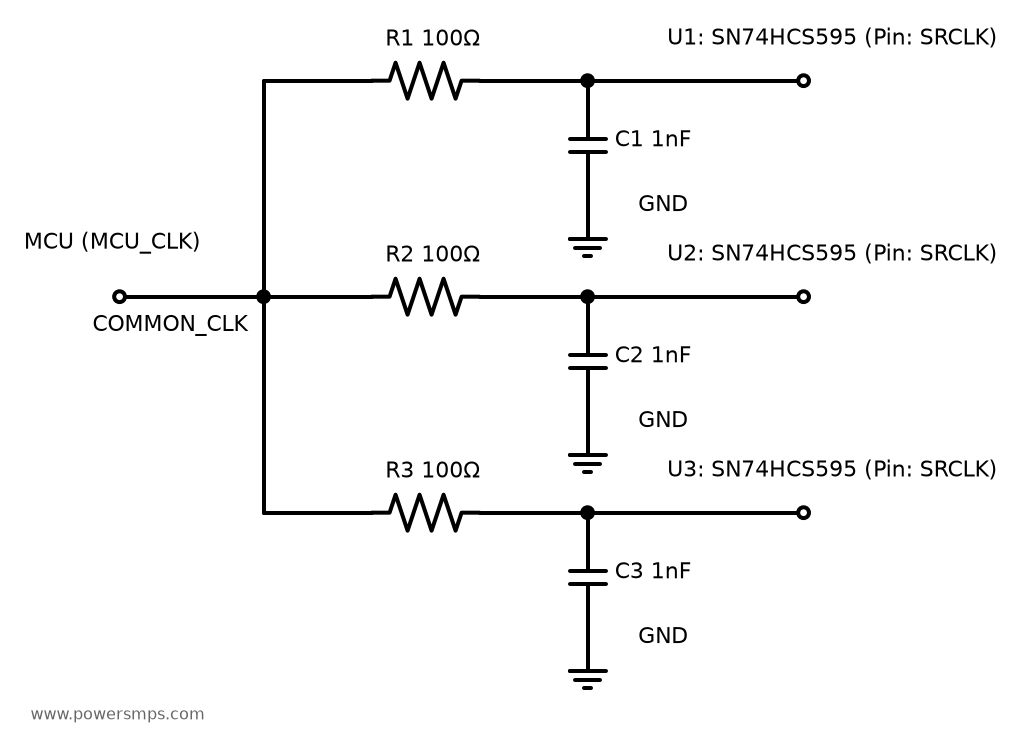
While retaining the SN74HCS595, we inserted a 100 Ω resistor in series with the CLK signal path and connected a 1 nF capacitor between GND and the SRCLK input node downstream of the resistor.
When distributing a common CLK to multiple ICs via stub traces, applying filters individually close to the CLK input of each IC proved effective. Because noise can also couple into traces downstream of the branch point, filtering at each receiving end is essential.
CLK branch 100 Ω series resistor and 1 nF filter between input and GND. The three branches represent an example configuration; DATA (SER), output latch (RCLK), power, and decoupling connections are omitted.
The schematic is a conceptual diagram illustrating the filter connections for each branch. The three branches represent an example configuration; DATA (SER), output latch (RCLK), power, and decoupling connections are omitted.
The connection sequence for each branch is Common CLK → 100 Ω series resistor → SRCLK input. The 1 nF capacitor connects from the input node downstream of the resistor to the local IC GND. Traces between the capacitor and GND should also be kept short.
The RC filter dampens voltage swings at the input node in response to short noise pulses, while the Schmitt trigger evaluates the filtered input signal against its hysteresis thresholds. The two countermeasures serve complementary roles.
Burst Test Results by Countermeasure
Implementation Stage
Observed Result
Existing 74595-series IC used
Output data shifted by 1 bit during burst testing
Replaced with SN74HCS595
Malfunction frequency reduced, but bit-shift symptom persisted
No bit-shift issues observed under test conditions
The above results were verified under test conditions where a 1 kV burst was applied to the AC power port in accordance with EN 55014-2. In this circuit, the symptom that remained after swapping the IC was resolved by adding the RC filter.
Timing Considerations When Applying to Other Circuits
The ideal RC time constant for 100 Ω and 1 nF is 100 ns. Although these component values resolved the issue in this circuit, the filter impacts not only noise but also the transition edges and arrival times of the valid CLK signal. Therefore, when adapting this solution to other circuits, the following items must be verified.
Valid CLK pulse width and input transition time: Verify that required clock conditions are still satisfied after filtering.
Data and output latch timing: Check the setup and hold times for SER, as well as the timing margin from the final SRCLK to RCLK, against datasheet specifications.
CLK arrival skew between multiple ICs: Account for skew caused by individual RC component tolerances and input threshold variations. In serial cascaded configurations in particular, verify data setup and hold margins between ICs.
MCU CLK output drive loading: As the number of branches increases, the cumulative capacitive load rises; review GPIO drive capability and actual signal transmission requirements.
The DRV10983 from Texas Instruments (TI) targets 12V to 24V systems as a 3-phase sensorless BLDC motor driver IC, driving motors with sinusoidal excitation without external Hall sensors. When implementing driver control and status diagnostics, selecting the FG (Frequency Generator) pin for rotational speed feedback and the current sensing methodology for load torque estimation are key design considerations.
1. Operating Principles of the DRV10983 FG Signal and RPM Measurement Mechanism
The FG (Frequency Generator) pin of the DRV10983 outputs digital pulses synchronized with the electrical rotation period of the motor rotor, serving as an interrupt source for real-time RPM measurement, closed-loop speed control, and motor stall/lock detection.
Open-Drain Interface Circuit
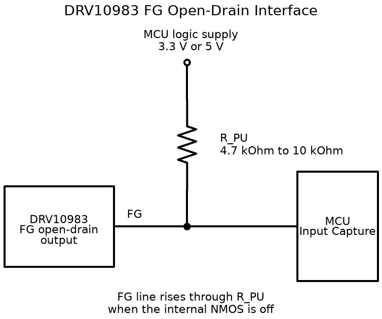
The internal output stage of the FG pin features an open-drain N-channel MOSFET structure. Because no internal pull-up resistor is integrated, an external pull-up resistor (\(R_{PU}\)) must be populated to pull the signal line to a logic high.
The supply rail for the pull-up resistor connects to the I/O logic level of the host MCU (+3.3V or +5V), with a recommended resistance range of \(4.7\text{ k}\Omega \sim 10\text{ k}\Omega\). If the resistance is excessively high, the PCB load capacitance delays the rise time of the square wave, causing pulse distortion at high rotational speeds; conversely, if it is too low, unnecessary sink current consumption increases in the low state.
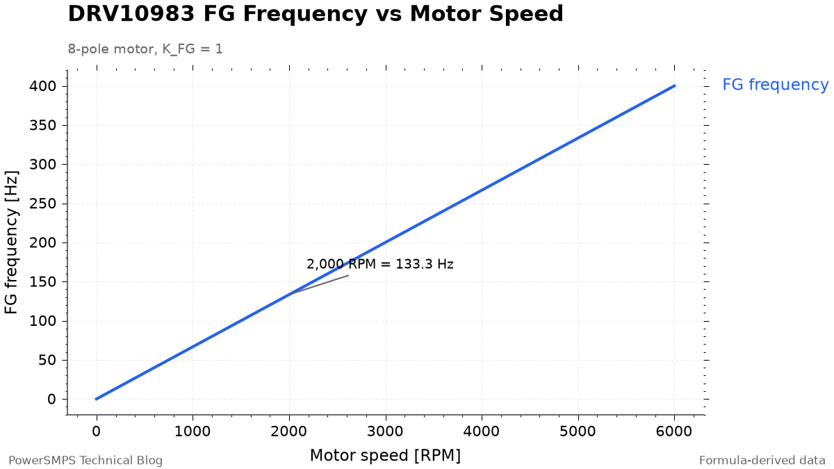
The frequency of the square wave output from the FG pin (\(f_{FG}\)) is proportional to the mechanical speed of the motor (RPM), the number of rotor poles (Poles, \(P\)), and the internal FGcycle register setting coefficient of the DRV10983 (\(K_{FG}\)).
\(P\): Motor pole count (number of poles; e.g., for an 8-pole motor, \(P=8\))
\(K_{FG}\): Output pulse scaling factor determined by the FGcycle register setting (controls electrical pulses per 1 revolution by default)
RPM–FG frequency relationship for an 8-pole motor with K_FG=1. Values calculated from formulas.
For an 8-pole (\(P=8\)) motor configured with \(K_{FG}=1\), per 1 mechanical revolution, 4 electrical cycles are generated, so operating at \(2,000\text{ RPM}\) results in an FG frequency of exactly \(133.3\text{ Hz}\).
2. Torque Estimation Limits of the FG Signal and the Necessity of Phase Current Sensing
When designing motor control firmware, confusion often arises regarding estimating load torque by monitoring changes in the FG pin frequency or duty cycle. However, the FG signal alone cannot determine motor load torque in the steady-state.
Physical Decoupling of Speed and Torque
The FG output signal purely provides information on the rate of change of the rotor electrical position—that is, mechanical speed alone. If the motor driver performs closed-loop speed control to maintain \(2,000\text{ RPM}\) constant, the FG pin output frequency remains identically \(133.3\text{ Hz}\) in both an unloaded no-load condition and a heavily loaded rated-load condition.
Although a temporary frequency drop can be observed during transient states when a sudden load step causes a speed dip, the frequency converges back to the target RPM once the speed loop restores steady-state, making it impossible to determine the magnitude of the steady-state load torque.
Phase Current (\(I_{phase}\)) as an Essential Requirement for Torque Calculation
The electromagnetic torque (\(T\)) of permanent magnet synchronous and BLDC motors is directly proportional to the product of the motor torque constant (\(K_t\)) and the active phase current (\(I_{phase}\)) flowing through the stator windings:
\[T = K_t \times I_{phase}\]
Even when maintaining a constant speed, as the load torque increases, the driver increases the applied voltage duty cycle to overcome back-EMF and generate torque, causing the motor winding current (\(I_{phase}\)) to rise proportionally. Therefore, to quantitatively measure motor output torque and load conditions, phase current or DC-link bus current data must be obtained.
3. Datasheet Revision Trap: MotorCurrent Specification Changes Between 2014 Rev and 2020 Rev H
When evaluating the current measurement capability of the DRV10983, the most critical hardware engineering risk is the issue of missing specifications depending on which datasheet revision is referenced.
Not provided (misleading users into believing I2C current monitoring is unsupported)
\(11\text{비트}\) piecewise conversion formula included
Revision History (Rev History)
–
“Added MotorCurrent1 and MotorCurrent2 to Register Map” explicitly stated
When consulting the early 2014 datasheet or referencing legacy PDF copies mirrored on unofficial archives, the 0x17 and 0x18 addresses in the register map are empty and marked as “Reserved,” easily leading to the erroneous conclusion that “the DRV10983 does not support internal current monitoring, necessitating an external shunt resistor and current sense amplifier circuit.”
However, in the official Rev H datasheet revised in 2020-5, the specifications for the 11-bit MotorCurrent[10:0] data registers derived through the internal ADC were officially established. Therefore, hardware designers must verify the register map based on the latest Rev H specifications.
4. Reading the MotorCurrent Register, Conversion Formulas, and Firmware Implementation Considerations
The DRV10983 calculates the motor peak current through internal sensing circuitry and an ADC, storing the result as an 11-bit digital value MotorCurrent[10:0] in the MotorCurrent1 (0x17) and MotorCurrent2 (0x18) registers.
Piecewise Current Conversion Formula
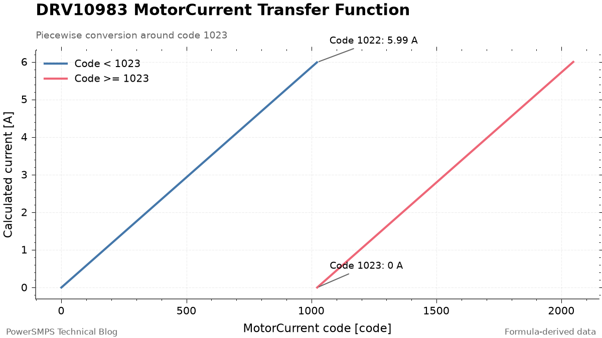
The formula for calculating the actual motor current (in A) from the 11-bit raw code (MotorCurrent[10:0], range: \(0 \sim 2047\)) features a piecewise structure bounded by code 1023:
When \(\text{MotorCurrent}[10:0] < 1023\):
\[\text{Current (A)} = \frac{3 \times \text{MotorCurrent}[10:0]}{512}\]
Piecewise conversion of the MotorCurrent 11-bit code and discontinuity at the 1022/1023 boundary. Values calculated from formulas.
Noise Spikes Near 0A and Firmware Filtering
The structural vulnerability of this conversion formula appears around code 1023. Under no-load or stopped conditions when the actual current is near 0A, around the internal calculation offset reference point of 1023, minute ADC noise on the order of 1 LSB causes a critical computational discontinuity:
When the code is \(1023\): \(3 \times (1023 – 1023) / 512 = 0.0\text{ A}\)
When noise causes the code to drop to \(1022\) by 1 LSB: Branch (2) applies, yielding \(3 \times 1022 / 512 \approx 5.988\text{ A}\)
In other words, during no-load operation, minute noise causes the calculated current to instantly jump from \(0\text{ A}\) to approximately \(6\text{ A}\). Left unaddressed, this leads to false overcurrent faults, speed-torque loop oscillation, and erroneous motor lock/stall detection.
Therefore, two processing stages are essential in firmware implementation:
1. Dead-band processing: Clamp LSB fluctuations within a specified range around code 1023 (e.g., in low-current regimes) to 0A.
2. Low-pass filter (LPF): Rather than using single-cycle sampled values directly, apply an 1-order IIR digital low-pass filter or a moving average filter to eliminate high-frequency spikes.
Necessity of 0x17-Initiated 2-Byte Burst Read
The 11-bit current data is stored across MotorCurrent1 (0x17, upper bits) and MotorCurrent2 (0x18, lower bits)—a total of 2 registers.
When reading this value via I2C communication, one must start from address 0x17 and perform an 2-byte continuous burst read. The internal register interface of the DRV10983 is designed such that the moment the master reads address 0x17, the lower byte value at address 0x18 is locked into an internal latch.
If I2C communication reads 0x17 and 0x18 in separate transactions or reads 0x18 first, the motor commutation timing may change between reading the upper and lower bytes, causing data corruption.
When configuring a motor control system, deciding whether to implement torque monitoring using the internal MotorCurrent register or by adding an external shunt resistor and current sense amplifier (CSA) circuit depends on system requirements.
Comparison Parameter
Integrated I2C MotorCurrent Approach
External Shunt + CSA (Current Sense Amp) Approach
Additional Components (BOM)
None (utilizes internal driver circuitry)
Requires shunt resistor, current sense amplifier, and passive filter components
PCB Footprint / Area
Minimal (no additional routing required)
Increased (requires area for shunt heat dissipation and Kelvin sensing traces)
Sampling Bandwidth
Low (I2C bus polling rate: tens to hundreds of Hz)
High (direct MCU ADC sampling: tens to hundreds of kHz)
Measurement Precision
Moderate (limited by internal ADC resolution and presence of 1023 discontinuity noise)
High (precision resistor tolerance and low-noise differential amplification)
Primary Applications
Simple overload monitoring, stall detection, fan/pump health monitoring
Selection criteria for integrated I2C approach: Recommended when motor torque control is not the primary objective, but rather overload shutdown protection, filter clogging detection, or qualitative load level determination. It can be implemented entirely via firmware algorithms without additional BOM cost or board area.
Selection criteria for external shunt sensing: Essential for industrial mechanisms requiring fast load response control on the order of sub-milliseconds (ms), high-precision torque ripple suppression, or transient current protection.