When using a 3.3V GPIO to control a 12V relay, you must first check the guaranteed on-resistance at the actual gate voltage rather than the MOSFET threshold voltage. Calculating the load current determined by power supply and coil tolerances, the drain peak voltage during coil turn-off, and the GPIO charge and discharge currents provides a clear rationale for component selection.
The following is a low-speed DC relay ON/OFF design example based on assumed operating conditions, not empirical measurements from a specific product.
Table of Contents
- 1. Check Guaranteed On-Resistance Instead of VGS(th)
- 2. Coil Current and Conduction Loss Calculations
- 3. GPIO, Gate, and Relay Interconnection Conditions
- 4. Series Gate Resistor and Pull-Down Calculations
- 5. MOSFET Voltage Rating Calculations with Coil Clamping
- 6. Distinguishing and Validating Low-Speed ON/OFF vs. PWM
1. Check Guaranteed On-Resistance Instead of VGS(th)
In the AO3400A datasheet Rev 3.1, the threshold voltage VGS(th) is defined under the conditions of drain current 250µA and VDS=VGS. The minimum, typical, and maximum values are 0.65V, 1.05V, and 1.45V, respectively. This test current is a conduction current used to define the threshold, not a condition that guarantees low on-resistance at relay load currents.
The manufacturer’s maximum on-resistance specifications are as follows. The junction temperature condition for the table is TJ=25°C.
| Gate Voltage VGS | Test Drain Current | Maximum RDS(on) |
|---|---|---|
| 2.5V | 3A | 48mΩ |
| 4.5V | 5A | 32mΩ |
| 10V | 5.7A | 26.5mΩ |
Even when using a 3.3V MCU, the GPIO High output is not always 3.3V. You must check the minimum VOH and load conditions in the MCU datasheet, and verify that VGS—accounting for voltage drops across the gate resistor network and source voltage fluctuations—is sufficiently higher than the test voltage specified in the on-resistance rating. Furthermore, the test currents in the on-resistance table must not be interpreted as allowable continuous currents on an actual PCB.
Source: AO3400A Official Datasheet, electrical characteristics and thermal characteristics tables.
2. Coil Current and Conduction Loss Calculations
The example conditions are assumed as follows. The GPIO values are not guaranteed specifications of any specific MCU.
| Item | Example Assumption |
|---|---|
| Nominal coil voltage and resistance | 12V·120Ω |
| Maximum supply voltage | 13.2V |
| Minimum coil resistance considering low temperature and tolerance | 108Ω |
| Minimum GPIO VOH | 2.9V |
| Gate charging current budget | 4mA |
| On-resistance used for calculation | 48mΩ, VGS=2.5V·TJ=25°C specification |
The nominal current is 12V/120Ω=100mA, and the assumed maximum current is as follows:
\[I_{coil,max}=\frac{13.2}{108}\approx0.12222\ \mathrm{A}\]Conduction loss is proportional to the square of current:
\[P_{cond}=I_{coil}^{2}R_{DS(on)}\]The calculated value at nominal current is 0.100²×0.048=0.00048W, or 0.48mW. Under the assumed maximum current condition, it is approximately 0.12222²×0.048=0.000717W, or 0.717mW.
This value is a conduction loss calculation applying the 25°C on-resistance. It is not a final guaranteed temperature value that includes on-resistance increases at high temperatures, switching losses, and actual PCB heat dissipation conditions. Because datasheet thermal characteristics are based on a 2oz copper, 1in² FR4 board in still air, actual board conditions must be verified separately.
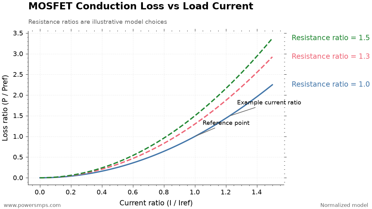
The resistance multipliers 1.0, 1.3, and 1.5 in the graph are model values chosen for comparison. They are not manufacturer-guaranteed values or measured data corresponding to specific temperatures. Under the same on-resistance, the graph shows the relationship where conduction loss increases by a factor of 1.44 when the current increases by a factor of 1.2.
3. GPIO, Gate, and Relay Interconnection Conditions
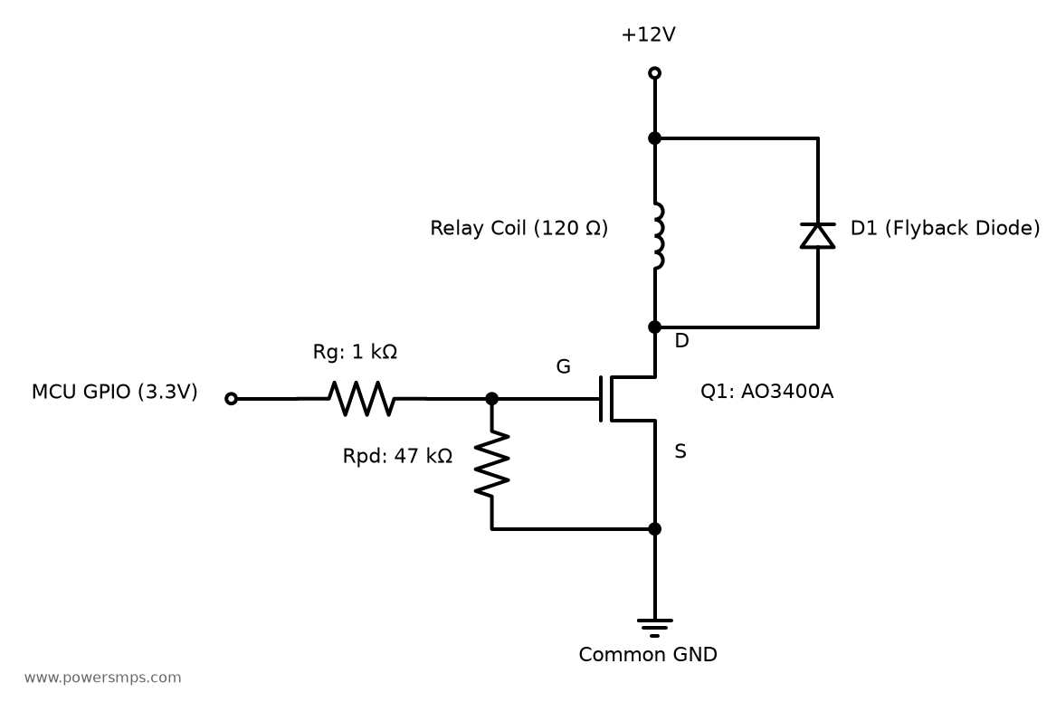
The example is a low-side N-MOSFET circuit where the MCU and load supply share a common ground. Connections are listed in the following table:
| Device / Node | Connection |
|---|---|
| Relay coil | Between +12V and Q1 drain |
| Q1 source | Common GND shared with MCU |
| Series gate resistor Rg | Between GPIO and Q1 gate, example value 1kΩ |
| Pull-down resistor Rpd | Between Q1 gate (downstream of Rg) and source, example value 47kΩ |
| Flyback diode D1 | Cathode to +12V, anode to Q1 drain |
The body diode of a low-side N-MOSFET conducts from source to drain. When the coil is turned off and the drain flies up to a positive voltage higher than the supply, the body diode is reverse-biased and cannot substitute for the coil flyback freewheeling path.
The relationship between diode ratings and relay release time can be further referenced in the previous article, Relay Flyback Diode Selection and Turn-Off Time Calculations.
4. Series Gate Resistor and Pull-Down Calculations
Modeling the GPIO as an ideal 3.3V voltage source and budgeting an initial gate charging current of 4mA, the lower limit calculation for the external series resistance is 3.3V/4mA=825Ω. In the example, 1kΩ is selected. Neglecting the GPIO internal output resistance, the calculated initial current upper limit is 3.3V/1kΩ=3.3mA. For actual component selection, verify both recommended source/sink currents and VOH/VOL conditions in the MCU datasheet. Never use the absolute maximum rated current as a continuous driving target.
Connecting a 47kΩ pull-down behind the gate creates voltage division in steady state. Under the conditions of minimum VOH 2.9V, negligible gate leakage, and a common ground without source voltage bounce, the calculation is as follows:
\[V_{GS}=2.9\times\frac{47}{1+47}\approx2.8396\ \mathrm{V}\]Under this DC assumption, the voltage is higher than the test voltage for the 2.5V on-resistance specification. In practical circuits, verify margin across temperature, supply tolerances, and source voltage variations. When the GPIO outputs 3.3V, the DC current flowing through the resistor network is 3.3V/48kΩ=68.75µA.
A static calculation is also possible for when the GPIO is High-Z during reset. Assuming a total leakage current of 1µA and an allowable gate voltage of 0.3V, Rpd≤0.3V/1µA=300kΩ. With 47kΩ, the static leakage voltage is approximately 47mV. While the pull-down should be placed close to the gate, this calculation does not guarantee prevention of false turn-on caused by Miller current injection during rapid drain voltage changes or across all power sequencing conditions.
5. MOSFET Voltage Rating Calculations with Coil Clamping
The absolute maximum VDS rating of the AO3400A is 30V. When selecting a device, adequate design margin must exist for the following voltage sum:
\[V_{sup,max}+V_{clamp,max}+V_{overshoot} < V_{DS,rating}\]Assuming a clamp voltage of 1V for a standard diode and a wiring overshoot of 3V, the peak is 13.2+1+3=17.2V. Although this is lower than 30V, this confirms only the assumed voltage sum, so actual drain waveforms and component tolerances must be verified.
Conversely, in an assumption combining a 24V Zener and a 0.8V forward-voltage diode, even without overshoot the sum is 13.2+24+0.8=38V. Therefore, the 30V AO3400A cannot be used under these conditions. When selecting higher voltage-rated devices, evaluate based on the Zener’s actual clamp current, temperature, tolerance, and wiring surges. Sizing MOSFET voltage rating based solely on supply voltage makes it easy to overlook this difference.
6. Distinguishing and Validating Low-Speed ON/OFF vs. PWM
The total gate charge Qg of the AO3400A is typical 6nC and maximum 7nC, but the test conditions are VGS=4.5V, VDS=15V, and ID=5.7A. This must not be used as a guaranteed charge value under 3.3V drive. Furthermore, Qg/Ig is a coarse charging time estimate and does not equal the actual drain transition time including the Miller plateau. For relevant principles, refer to the TI SLUA618A Gate Driver Design Document.
Do not apply resistor values for low-speed relay ON/OFF directly to high-speed PWM solenoid circuits. Whether a dedicated driver is required should be determined by examining gate charge, GPIO source/sink capability, switching losses, temperature, and the EMI budget together.
The final verification sequence is as follows:
- Recalculate maximum current using actual component coil tolerances and supply voltage ranges.
- Measure gate-to-source voltage during normal operation to verify it meets the on-resistance guarantee condition.
- Check for spurious gate turn-on and source voltage bounce during boot, reset, and power-up sequencing.
- Verify that the drain peak and ringing during coil turn-off remain within the selected breakdown voltage margin.
- Check heat dissipation on the actual PCB and at operating temperatures.
The core sequence is Verify guaranteed on-resistance at actual VGS → Calculate maximum coil current and losses → Validate gate resistor network → Verify VDS including clamp. The 1kΩ and 47kΩ in this example are a starting point calculated under these conditions, and must be reconfirmed against the datasheets of the MCU and relay to be used.
Leave a Reply