The high voltage generated when interrupting current through a coil and the principle by which a buck converter maintains load current while repeatedly switching are fundamentally identical. Both phenomena can be explained by the inductor’s core characteristics: generating a voltage in response to changes in current, and storing energy in its magnetic field.
A coil refers to a structure of wound wire, whereas an inductor is a circuit component that utilizes the inductance of that structure. A relay coil uses magnetic force to actuate mechanical contacts, while a power inductor transfers energy and controls current ripple throughout the switching cycle. This article connects both applications through fundamental equations.
Table of Contents
1. How Does an Inductor Oppose Current Change?
The unit of inductance \(L\) is the henry (H), with mH and µH also widely used in circuits. An ideal inductor with constant inductance obeys the following relationship:
\[v_L=L\frac{di}{dt}\]This equation applies the passive sign convention, where the terminal into which current enters is defined as positive (+). For a given applied voltage, a larger \(L\) results in a smaller rate of current change \(di/dt\). When the voltage is positive, the current increases; when negative, the current decreases. In this model with finite applied voltages, current cannot jump instantaneously to a different value.
In electromagnetism literature, the induced electromotive force (EMF) from self-induction is often written as \(\varepsilon=-L\,di/dt\). The negative sign signifies that the induced EMF has a polarity opposing the change in current. In circuit theory under the passive sign convention, the terminal where current enters is defined as positive (+), yielding a terminal voltage of \(v_L=-\varepsilon=L\,di/dt\). When the reference directions for terminal voltage and induced EMF are properly distinguished, the two expressions are fully consistent.
In DC steady state, the current is constant so \(di/dt=0\), and the voltage across an ideal inductor is 0V. In a practical inductor, the winding DC resistance (DCR) causes a voltage drop of \(I\times\mathrm{DCR}\) and a power loss of \(I^2\times\mathrm{DCR}\). It is essential to distinguish the transient current change before reaching steady state from the resistive loss after reaching it.
2. How Much Energy Is Stored in the Magnetic Field?
In a linear model with constant inductance, the stored energy is expressed as follows:
\[E=\frac{1}{2}LI^2\]This is obtained by integrating \(p=v_Li\). For a constant inductance, doubling the current quadruples the stored energy. In regions where core saturation causes \(L\) to vary significantly with current, this equation with constant \(L\) cannot be directly applied.
As an educational example, substituting \(L=10\,\mathrm{mH}\) and \(I=0.1\,\mathrm{A}\) yields the following:
\[E=\frac{1}{2}\times0.01\times0.1^2=50\,\mu\mathrm{J}\]This calculation is based on an idealized linear model; when the switch turns off, this energy does not vanish, but is instead transferred to another path or dissipated as heat across resistance and protective components.
3. Relay Back EMF and Flyback Diodes
Consider driving a DC relay with a low-side MOSFET. When the switch turns ON, current flows along the path: Supply → Coil Top → Coil Bottom → MOSFET → GND. Once fully settled, the current is determined by factors including the supply voltage and coil resistance.
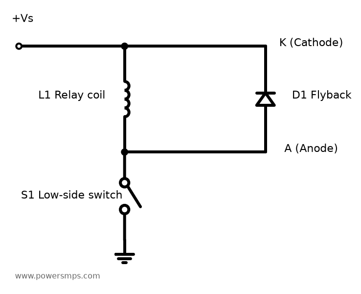
When the switch turns OFF, the path through the MOSFET is interrupted, but the coil current cannot instantly drop to 0. The coil reverses its voltage polarity to maintain the existing current direction. In low-side drive where the coil top is tied to the supply, the bottom node—the drain—can rise well above the supply voltage. Without an adequate protection path, this overvoltage can exceed the switch ratings and cause damage. The peak voltage and damage risk depend on stored energy, parasitic components, and device avalanche ratings.
Diode Orientation and OFF Current Path
A flyback diode is connected in parallel with the coil:
- Cathode (K): Connected to the positive (+) supply at the top of the coil. This corresponds to the banded side of a typical diode package.
- Anode (A): Connected to the bottom of the coil and the switch drain node.
While the switch is ON, the diode is reverse-biased. After the switch turns OFF, the rising voltage at the bottom of the coil forward-biases the diode, establishing a circulating freewheeling loop: Coil Top → Coil Bottom → Diode Anode → Cathode → Coil Top. Current within the coil does not suddenly reverse direction.
In a simplified model excluding overshoot caused by trace parasitics, the drain voltage relative to ground is clamped to approximately:
\[V_{\mathrm{drain}}\approx V_s+V_F\]Here, \(V_F\) is the forward voltage of the diode at the operating current and temperature. In practical circuits, transient voltage overshoot from layout parasitic inductance can add to this value; therefore, both the peak drain voltage and the MOSFET voltage rating margin must be verified alongside this approximation.
Why Does Adding a Diode Delay Relay Release?
A lower clamping voltage reduces switch voltage stress, but extends the time required for current to decay. Modeling the coil as a series combination of constant inductance \(L\) and winding resistance \(R\), and approximating diode forward drop during conduction as \(V_F\), yields the following equations:
\[L\frac{di}{dt}+Ri=-V_F\] \[\frac{di}{dt}=-\frac{Ri+V_F}{L}\]The total top-to-bottom coil terminal voltage is approximately \(-V_F\), while the voltage across the ideal inductance element alone is \(-(Ri+V_F)\). Only when winding resistance is neglected does this simplify to \(di/dt=-V_F/L\).
A simple parallel diode results in slower demagnetization compared to clamping schemes operating at higher voltages, thereby lengthening relay release time. In practice, contact release time is governed not only by coil current decay, but also by magnetic properties and mechanical dynamics including return spring forces. When faster release is required, Zener diode or TVS clamps are evaluated, provided that the switch breakdown voltage and clamp energy ratings are properly verified. Specific component selection is examined in detail in Flyback Diode Selection and Relay Release Time.
This DC parallel diode configuration must never be applied directly to AC coils, because the diode would conduct heavily during one half-cycle. For AC loads, appropriate suppression methods such as RC snubbers, MOVs, or bidirectional TVS diodes must be evaluated according to ratings and operating conditions.
4. How Does an Inductor Operate in a Buck Converter?
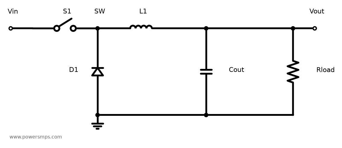
A buck converter is a switching power supply that generates a DC output voltage lower than its input. Here, we assume ideal steady-state continuous conduction mode (CCM), neglecting losses, with an output voltage that remains virtually constant across the switching cycle and an inductor current that stays strictly positive. Inductor current reference is defined from switching node SW to the output, and inductor voltage is defined as the voltage at SW minus the output voltage.
| Interval | Current Path | Inductor Voltage | Current Trend |
|---|---|---|---|
| High-Side Switch ON | Input → High-Side Switch → Inductor → Output → GND | \(V_{in}-V_{out}\) | Increase |
| High-Side Switch OFF | GND → Freewheeling Diode or Conducting Low-Side MOSFET → Inductor → Output → GND | \(-V_{out}\) | Decrease |
During the ON interval, the input delivers energy to the load while stored energy in the inductor increases. During the OFF interval, the inductor’s stored energy decreases as it continues supplying current to the output. In a synchronous buck converter, the controller drives the low-side MOSFET to form this freewheeling conduction path.
Using switching period \(T_s\) and duty cycle \(D\), the steady-state inductor voltage satisfies the volt-second balance principle:
\[(V_{in}-V_{out})DT_s-V_{out}(1-D)T_s=0\]Consequently, under ideal CCM conditions, the following relationship holds:
\[D=\frac{V_{out}}{V_{in}}\]Calculating Ripple Current and Peak Current
The inductor current alternates between rising and falling around its average value. The peak-to-peak ripple current is given by:
\[\Delta I_{pp}=\frac{(V_{in}-V_{out})D}{Lf_s}=\frac{V_{out}(1-D)}{Lf_s}\]where \(f_s=1/T_s\). In steady state, the average inductor current equals the output load current, while the output capacitor absorbs most of the ripple component to minimize output voltage variations.
\[I_{pk}=I_{out}+\frac{\Delta I_{pp}}{2},\qquad I_{min}=I_{out}-\frac{\Delta I_{pp}}{2}\]For an educational calculation example, assume an input of 12V, output of 5V, switching frequency of 100kHz, inductance of 100µH, and output current of 1A.
| Calculation Parameter | Result |
|---|---|
| Duty cycle \(D=5/12\) | Approx. 0.417, or 41.7% |
| Period \(T_s=1/f_s\) | 10µs |
| Ripple current \(\Delta I_{pp}\) | Approx. 0.292App |
| Peak current \(I_{pk}\) | Approx. 1.146A |
| Valley current \(I_{min}\) | Approx. 0.854A |
Since the valley current is greater than 0, this calculation is consistent with the CCM assumption. The waveforms below illustrate these identical conditions computed from the mathematical model.
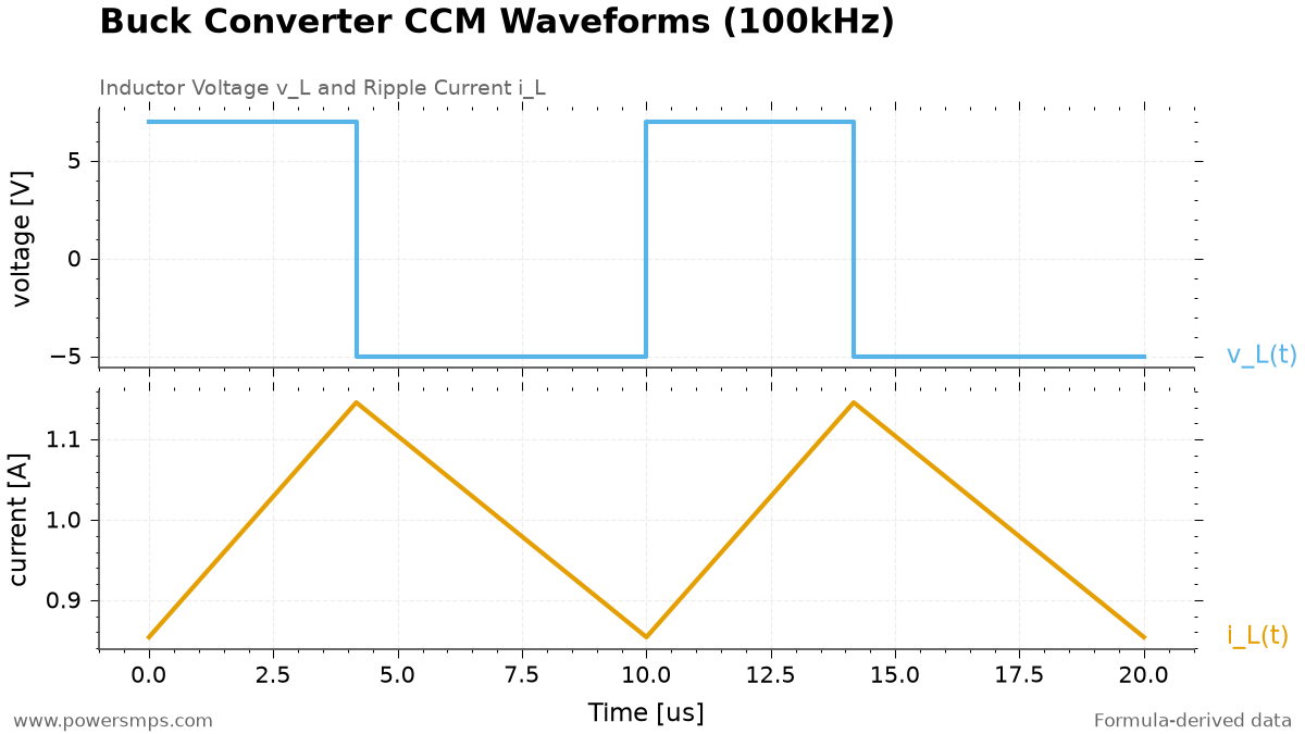
When the load decreases such that the inductor current drops to 0 and reverse current is blocked, the converter can enter discontinuous conduction mode (DCM) where an interval with 0 current occurs. Under DCM, the simple conversion ratio above is no longer directly applicable. Conversely, a forced-CCM synchronous buck converter can allow negative inductor current at light loads, so light-load operation does not necessarily imply DCM.
5. Beyond Inductance (L): Key Ratings for Real Inductors
| Parameter | Significance | Value to Compare in Circuit |
|---|---|---|
| Inductance \(L\) and Tolerance | Affects rate of current change and ripple | In-circuit L accounting for DC bias, temperature, and tolerance |
| Saturation Current \(I_{sat}\) | Current at which L drops by a manufacturer-specified percentage from its zero-bias value | Worst-case peak current |
| Temperature Rise Current Rating \(I_{rms}\) | Current producing a specified temperature rise under manufacturer test conditions | RMS current of the actual waveform and operating environment |
| DCR | DC resistance of the winding | Voltage drop and \(I_{rms}^2\mathrm{DCR}\) loss |
| Core and AC Winding Losses | Losses caused by switching flux swing and AC current | Manufacturer loss data under frequency, ripple, and temperature conditions |
The saturation current rating is not a threshold where current cuts off or the device instantly fails; rather, it is the benchmark at which inductance drops by a specified percentage. Designers must check the manufacturer’s defined inductance rolloff criteria and verify how much L is maintained under operating temperature and peak current conditions. If L decreases, the current changes more rapidly under the same voltage, which can increase ripple and peak currents.
The temperature rise rating is likewise determined under standardized laboratory test conditions and does not directly guarantee component temperature in an actual operating environment. Ambient temperature, PCB thermal dissipation, and AC losses must be evaluated collectively. When selecting components, carefully verify and compare the specific test conditions and inductance drop percentages specified for \(I_{sat}\) and \(I_{rms}\) in the datasheet.
The RMS value of the triangular current waveform in the CCM model above can be calculated as follows:
\[I_{L,rms}=\sqrt{I_{out}^2+\frac{\Delta I_{pp}^2}{12}}\]Component selection must account not only for nominal load, but also for input voltage range, startup and load transients, IC current limits, and inductance tolerances. Because DC losses from DCR alone cannot account for core losses and AC winding losses, consult manufacturer loss modeling tools and verify actual operating temperatures.
6. Connecting the Three Applications
When turning off a relay, one must provide a freewheeling path for coil current and safely handle the stored energy. In a buck converter, the same property of current continuity is leveraged to sustain continuous output current between switching states. In both cases, the foundational starting point is the linear inductor relationship: voltage governs the rate of current change, and stored energy is proportional to the square of current.
When reviewing circuit designs, it is advisable to verify the following checklist:
- Are the relay coil OFF current path and diode polarity correctly oriented?
- Does the protection scheme satisfy both clamp voltage limits and relay release time requirements?
- Do the circuit conditions match the buck converter design assumptions (CCM, steady state, lossless)?
- Have in-circuit inductance (L), peak current, RMS current, operating temperature, and total losses all been verified?
For detailed selection of relay driver switches, refer to 3.3V MCU Relay Driver MOSFET Selection; for passive component fundamentals, see Capacitor Basics and Resistor Basics.
References
- Texas Instruments — SNVAA45: Inductive Load Turn-Off and Demagnetization
- Texas Instruments — SLVA949: Inductive Load-Switching Off Clamp
- Texas Instruments — Basic Calculation of a Buck Converter’s Power Stage
- Analog Devices — Buck Power Stage Design Equations
- Coilcraft — Current and Temperature Ratings
- OpenStax — University Physics Volume 2: Self-Inductance and Inductors
- OMRON — FAQ02129: Surge Suppression for Inductive Loads and Zener Diode Series Clamp
- OMRON — FAQ02804: Relay Release Delay Comparison by Surge Suppression Circuit
- OMRON TECHNICS — Dynamics simulation technology for high electrical durability relay
- Infineon — Power MOSFET avalanche design guidelines
- NIST — SI Units: The Henry (H) for Inductance
- Coilcraft — Inductor DC Resistance (DCR) and Voltage Drop
Leave a Reply